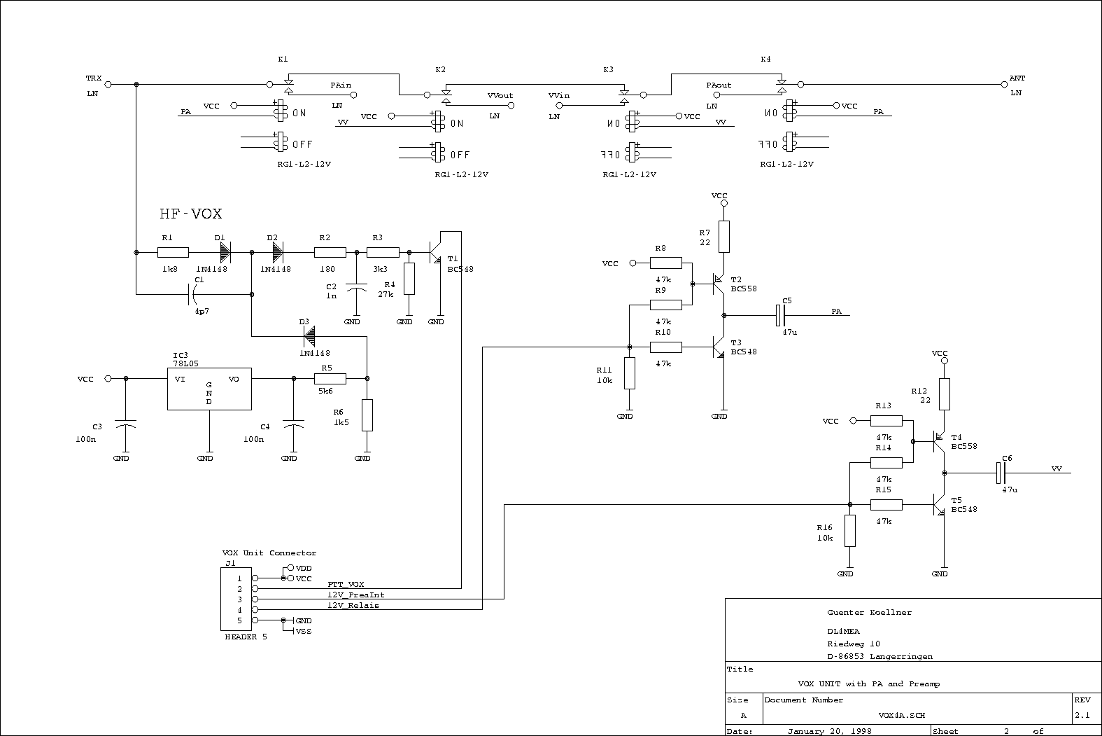
D: Diese Schaltung ermöglicht die Sende-/Empfangsumschaltung einer beliebigen PA auf Frequenzen bis zu 23cm. Weiter habe ich für den Empfangspfad einen beliebigen Vorverstärker vorgesehen. Die Schaltung verwendet im Moment bistabile Relais, aber mit wenigen Änderungen (Weglassen einiger Bauteile) können auch monostabile Relais verwendet werden.
Erklärung der Schaltung:
Von dem vom Sender kommenden HF-Signal wird über C1 ein geringer Teil ausgekoppelt. Eine eventuell vorhandene Schaltgleichspannung wird über R1/D1 erfaßt und ebenfalls benutzt. Der Transistor T1 ist über die mit Hilfe von IC3/R5/R6 erzeugte Vorspannung bereits kurz vorm Durchsteuern, weshalb bereits eine geringe Leistung ausreicht, um das Ausgangssignal zu erzeugen.
Die Relais K1 und K4 schalten die HF-Leistung auf die Sendeendstufe. Im Empfangspfad liegen K2 und K3 und schalten einen Vorverstärker. Die im Schaltplan erwähnten RG1-L2-12V sind bistabile Relais und lassen sich durch die verwendete Gegentakt-Schaltung von T2/T3 und C5 bzw. T4/T5/C6 schalten. Lediglich die Ruhelage ist nicht bestimmt und entsteht möglicherweise erst nach dem ersten Schalten. R7 und R12 schützen die Transistoren bei möglicherweise gleichzeitigem Durchschalten.
Verwendet man monostabile Relais, z.B. RG1-12V, kann R7, R8, R9, T2 entfallen, C5 wird überbrückt, gleiches bei R12, R13, R14, T4 und C6.
Das Relais K4 muß bei ist auf max. 10W begrenzt. Ich empfehle auf 144MHz bei Leistungen über 40W, 432MHz über 20W und 1296MHz über 10W dieses Relais durch ein Koaxrelais zu ersetzten, beispielsweise durch ein Relais mit 2*RG58 und einmal N-Buchse, das dann direkt an die Rückwand montiert wird.
Die Auswertung des Ausgangssignals bzw. Ansteuerung der Relais muß eine separate Schaltung übernehmen. Dazu gibt es zwei Varianten:
E: This circuit is used as a receive-/transmit-switch for any power amplifier for frequencies up to 23cm. Further there is a switch for any kind of receive preamplifier in the receive path. The relays being used are bistable, but the circuit can also be equipped with monostable with a few modificatons (just leave away some parts).
Circuit Description:
A small part of the TX's signal is taken by C1 and reticified. A possible present switching voltage is detected by R1/D1 and used to switch the VOX, too. T1 is short before switching because IC3/R5/R6 hold it on a low DC level. Doing so, a small amount of RF voltage is enougth to switch the output signal.
The relays K1 and K4 are used to switch the RF power to the output amplifier. In the receive path K2 and K3 allow to use a receive preamplifier. The RG1-L2-12V relays mentioned in the circuit diagram are bistable relays, so the push-pull circuit around T2/T3/C5 (T4/T5/C6 resp.) allows to swich them. Only the initial connection is not defined and might be present just after the first switching. R7 (R12 resp.) protects the transistors from a high current in case that both are on at the same time.
If you use monostable relays, for example RG1-12V, you may leave out R7, R8, R9 and T2 (R12, R13, R14, T4 and C6 resp) and just bridge the capacitors.
The relay K4 is rateted to 10W. I suggest to replace it by a coax relais when running more than 40W on 144MHz, 20W on 432MHz and 10W on 1296MHz. Preferably a relay with 2*RG58 and 1*N-connector should be used, which can easily mounted on the back side of the cabinet.
The output signal and relay control signal is produced in a separate circuit. There are two different ones:
Last Minute Information:
If you use a bistable relais for K2 (preamp to transceiver) then when you switch off the PA with the preamp on this relais would stay in its position and can never change again. So when the TRX transmits, the power is fed into the preamp. Mine blew doing so. A solution is to add a diode plus large capacitor at the circuits power supply so that it still has power to switch when all around is powered off. Tried and verified.
Schematic: (click on the image to view (and save) a high resolution GIF picture)
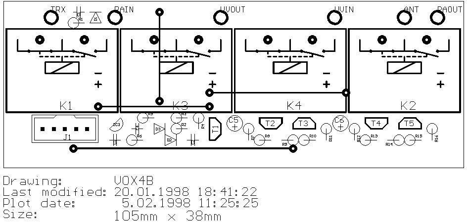
Picture: Place Plan (click on the image to get a Postscript file)
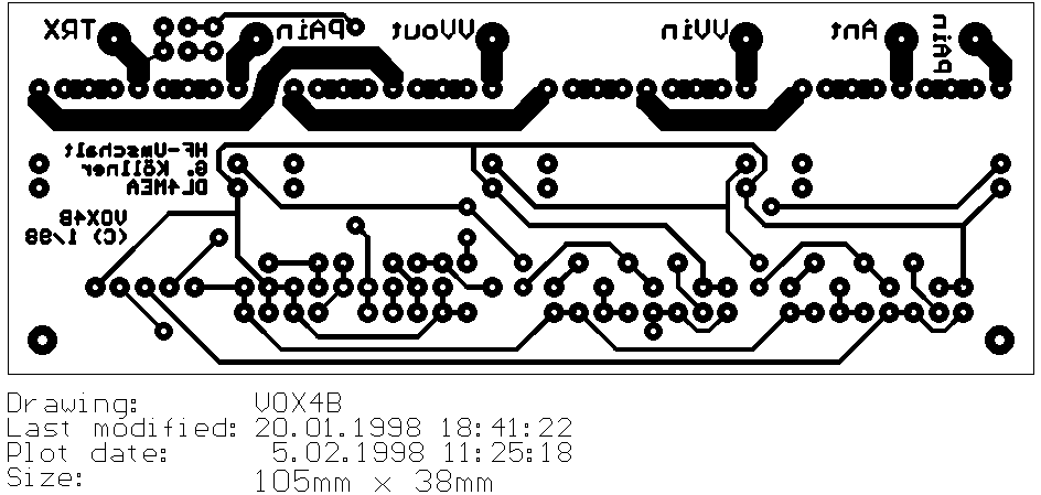
Picture: Solder Side (click on the image to get a Postscript file)
![[HOME]](green.gif) Last updated 980127 08:00 by DL4MEA
Last updated 980127 08:00 by DL4MEA