GPSDO with ADC and programmable frequency output

File:   ?\pic\GPSDO\html\gpsdo_pic.htm
Web:    www.qsl.net/dl4yhf/gpsdo/html/gpsdo_pic.htm
Author: Wolfgang Büscher, DL4YHF
Date:   2016-02-21

Under construction !


This file descibes the PIC microcontroller firmware for a GPS-disciplined oscillator (GPSDO). It is closely related with the sourcecode (gpsdo_pic_main.c), available on the author's website (see links above).

Details are in the sourcecode itself; this document actually links into it.
Those links into the sourcecode (mainly "C") only work if the sources are located in the same directory as this document. The sources also 'link back' into this file, when loaded with an HTML browser.

Contents

  1. Functional description
    1. Principle
    2. Block diagram (circuit)
    3. Prototype board (with PIC16F1783)
  2. Operation
    1. LED indicators
    2. Analog input
    3. Command interface
  3. Notes from the firmware development phase
    1. The development system
      1. Installing MPLAB and the C compiler
      2. A few rants about the development system
    2. Flashing (downloading) the firmware into the chip
    3. Details about the PIC16F1783
      1. Timer Capture (for the GPS sync pulse input)
      2. The PSMC (Programmable Switching Mode Controller)
  4. Appendix
    1. Links (external)
    2. Disclaimer

1. Functional description


1.1 Principle


1.2 Block diagram (circuit)


1.3 Prototype board (with PIC16F1783)


2. Operation


2.1 LED indicators


2.2 Analog input


The PIC16F1783 microcontroller in the first GPSDO variant has a built-in 12-bit A/D converter, which may replace the soundcard if the ADC's sampling rate permits. The datasheet specifies a maximum of 75 kSamples/second; but obviously only at 10 bit resolution. In the final version of the PIC firmware, the ADC now delivers 50 kS/sec, which are then decimated with appropriate digital low-pass filtering (actually using a 4th-order CIC filter to decimate by four). The final output (sent to the PC over a serial interface) is 12.5 kHz.
Note:
With an input sampling rate of 50 kHz, signal components above the Nyquist frequency limit (fs/2, i.e. 25 kHz) must be removed with an analog lowpass filter to avoid aliasing. Since the maximum (theoretical) frequency component in the output (at fs_out = 12.5 kHz) is limited to 6250 Hz anyway, the analog filter's frequency response doesn't need to be very steep:
The transition from pass- to stopband may be anywhere between the maximum signal frequency (required by your application, e.g. 6 kHz) and 25 kHz.
By deliberately not cutting off everything above 25 kHz, the PIC can be abused as an LF receiver. For example, by connecting a bandpass centered at 77.5 kHz between an antenna and the PIC's analog input, the GPSDO can be (ab-) used as a direct low-frequency receiver for the german DCF77 time signal transmitter. By subsampling the 77.5 kHz signal with fs_in = 80 kHz, the 'radio frequency' is converted down to (80 - 77.5 =) 2.5 kHz. This is possible because the PIC's analog uses a fast-acting Sample and Hold circuit. Of course, the S & H wasn't intended as an 'RF downconvter', but for a frequency stability test (by plotting the DCF77 phase from the subsampled 77.5 kHz signal) the sensitivity was sufficient.
Figure 1: GPSDO abused as a crude 'direct conversion' receiver, DCF77 carrier phase plotted at night, with ground/skywave interference

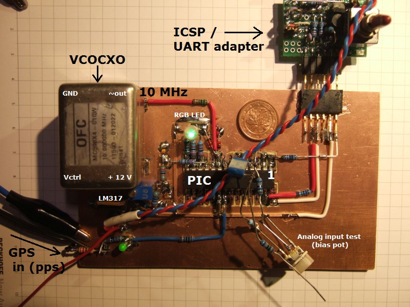
The output of the CIC filter, decimated to fs_out = 12.5 kSamples/second, can be sent via the PIC's serial port. Samples are sent with 16 bit per sample, because the decimation-by-four increases the resolution to more than the 12 bits from the ADC (with 'dithering noise' being always present with real signals). In addition to the 16 bits per sample, each sampling frame contains an additional byte for sychronisation, and to deliver additional information from the GPSDO to the receiving PC (details in a future chapter).
The baudrate is fixed to 500 kBit, which is far below the maximum a modern USB <-> RS422 or RS323 adapter can handle. With a FTDI-chip-based USB (2.0) to 'RS-232' adapter ("Delock USB 2.0 to serial"), this baudrate worked perfectly, and during a long test run (plotting the phase of the subsampled DCF77 signal over many hours), not a single byte was lost on the serial port.

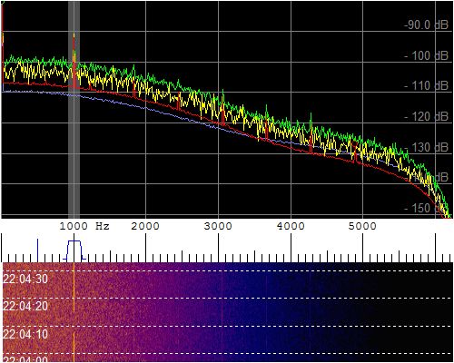
Figure 2: Input noise of the analog input, with a 1 kHz 0.1 mVpp test signal (-90 dBfs).
FFT bin width ~ 0.8 Hz (12500 Hz / 16384 points).
Green: Peak holding graph. Red: Long term average. Yellow: Momentary spectrum. Blue: Averaged spectrum with input fed with 'DC'.
Passband droop of the CIC filter not compensated here yet.


2.3 Command interface


To keep the (PIC16F1783-)firmware as simple as possible, 'commands' sent from the PC to the GPSDO are limited to single characters. At the time of this writing, the following 'commands' existed:

3. Notes from the firmware development phase


This chapter is intended for users which want to modify the firmware.
It is not necessary to read and understand this chapters to just use the GPSDO.

3.1 The development system

To develop and test the PIC firmware, all you need is a text editor, an a 'toolchain' to compile the sourcecode into object code, link the object code into a hex file, and a programmer to download the hex file into the target a couple of times each day.
The required software used to be available for free from the Microchip site (see links), even though the 'free' edition of the C compiler has its limitation, and will keep bugging you with a message like the following:
Warning [1273] ; . Omniscient Code Generation not available in Free mode
  (...)
You have compiled in FREE mode.
Using Omnicient Code Generation that is available in PRO mode,
you could have produced up to 60% smaller and 400% faster code.
See http://www.microchip.com/MPLABXCcompilers for more information.
Fortunately much of the "C" code is only used for initialisation, and since up to now there are no really time-critical parts in the program, it doesn't matter much if the code "could be 400% faster" (it's a bit hard to believe why a chip manufacturer makes a development tool, which can only be used to develop code for their own product (PICs) so inefficient - see 'rants' in a later chapter.
Anyway, if you ever programmed PIC16Fxx(x(x)) in Assembler, you will love not having to care about the goddamned register banks yourself anymore - the compiler inserts code to set the bank selection bits automatically, and even the free C compiler edition seems to do this job properly.

3.1.1 Installing MPLAB and the C compiler

IDE: Find, download, and install MPLAB v8.85 from the Microchip website.
This is an older version, but it could be convinced to work with the XC8 compiler.
If you have a really fast PC and like a flashy overloaded IDE, try MPLAB-X instead.

Compiler: If not already contained in the 'IDE', install Microchip's C compiler, too.
For the PIC16 family, the compiler is 'XC8'. The original firmware (hex file) was built with MPLAB XC8 C Compiler (Free Mode) V1.35. Later versions may work but were not tested.

3.1.2 A few rants about the development system

Being used to the simple, clean, but hopelessly outdated versions of Microchip's PIC development system (MPLAB), the recent 'recommended' version (which supports the newer chips) was quite a shock. Below are a few snippets collected from various sites (which confirms that non-believers in MPLAB-X are not alone).
   > How do you turn off ALL of the 'clever' formatting in MPLABX's editor ?
   > It seems like it took me forever to get MPLABX to stop doing stuff I didn't want it to do.
   > I would like the cursor to stay where I put it when start typing.
No much to add to that quote from a PIC forum. Don't waste your time on it - you simply cannot turn off that annoying feature (at least not in "MPLAB-X IDE V3.15", anno 2015). But for debugging, we are doomed to use MLPAB X, because MPLAB 8 still cannot keep sourcecode lines and breakpoints in sync while debugging, as soon as subroutines (or functions in C) are called... aaargh !

Solution: Edit in Notepad++ or MPLAB 8, and debug in "MBLAB X".
Another quote from a PIC forum:

Where is the "MPLAB-X" project file to "build" the firmware with ?
   There is no project file. MPLAB-X makes everything as complicated
   and obfuscated as possible :
   > When you try to open a project with MPLAB X, every directory you select 
   > (in the file browser opened via File->Open project for example) looks for
   > an nbproject subdirectory which contains all the 'project' files. 
   > There are file such as configurations.xml, etc that tell MPLAB X that 
   > this folder is an MPLAB X project.
   (..)
   > When you create a project in MPLABX, none of the files that it creates 
   > can be used to open MPLABX. Instead, you have to open MPLABX and then 
   > open your project by navigating to it (or leave it open in MPLABX when you 
   > close the IDE). 
   (..)
   > (MPLABX is based on Netbeans version 6, so I imagine something similar 
   >  could be done to open Netbeans projects. I'm not familiar with the
   >  native Netbeans or other types of Netbeans projects, so I'm just guessing here.)
NETBEANS ? JAVA-BASED IDE ? That explains why MPLAB-X is such a sluggish, bulky monster !
(but, unlike MPLAB, breakpoints and sourcecode-lines are in sync in MPLAB-X,
which never worked in MPLAB as soon as subroutines were called. )
On the author's few-years-old PC, MPLAB v8.85 (an older version, which could be convinced to work with the XC8 compiler) compiled and linked the entire project within fractions of a second.
MPLAB-X (the bulky, JAVA-based monster) required several minutes to load and initialize the project, was 'unable to generate the disassembly listing file', and required the fastest PC (fast CPU with several gigabytes of RAM) to achieve an acceptable speed while single-stepping in the debugger (simulator).
At least, the simulator's various 'Debugging' and 'PIC Memory' windows were quite helpful during the debugging phase.

3.2 Flashing (downloading) the firmware into the chip

If you already have a PIC programmer (or even one of Microchip's in-circuit programmers or debuggers), use them. If, years ago, you invested (a lot) in Microchip's Picstart/Picstart Plus, you're out of luck because that programmer doesn't support any of their recent chips (including the PIC16F17xx family).

With a few discrete standard components (no ICs) you can build your own in-circuit PIC programmer. The author used his own ('DL4YHF Serial Programmer V2'), which can be used as a terminal interface for debugging (after programming), because the PIC's in-circuit-programming pins can be used as UART TXD / RXD, in other words be connected to a standard serial port.


3.2 Details about the PIC16F1783


3.3.1 Timer Capture (for the GPS sync pulse input)

To achieve the lowest possible phase noise (jitter), the timing of the GPS sync pulses (to measure the OXCO frequency and phase relative to the initial 'lock') needs to be measured with the greatest possible resolution. The following text quoted from the PIC16F1783's datasheet (PIC16(L)F1782/3 DS40001579E page 2) caught the author's eye:

 * Two Capture/Compare/PWM modules (CCP):
    - 16-bit capture, maximum resolution 12.5 ns
12.5 nanoseconds timer capture resolution for a chip with a maximum specified clock frequency of 32 MHz ? Whow, almost too good to be true, because 12.5 ns would mean the timer (connected to the capture unit) could run at 80 MHz input clock.
Unfortunately the datasheet doesn't give a clue how. Later, thus turned out to be the usual "marketing guerilla" announcement which makes a lot of unfair assumptions to make the info on the first datasheet pages 'look nice'.
In fact, the PIC16F178x's CCP (Capture/Compare unit) is always synchronized to ONE INSTRUCTION CYCLE, which, as in the PIC stoneage, is still just A QUARTER of "Fosc".
With a 'slightly overclocked' PIC (Fosc=40 MHz, Fcyc=10 MHz instead of the allowed Fosc=32 MHz, Fcyc=8 MHz), the real capture resolution (without taking the prescaler into account!) is 1 / Fcyc = 100 nanoseconds. That's not spectacularly good (considering the fact that many GPS receivers can control the position of their sync output pulse with a granularity of 40 ns or even better), but on first glance (in 2015) it was used as a start -
  last not least because a bunch of PIC16F1783's had already been bought.

            -> May have to try a dsPIC30, not dsPIC33, instead...
               more on that in C:\pic\GPSDO_dsPIC\GPSDO_dsPIC.c .

3.3.2 The PSMC (Programmable switch-mode controller in PIC16F1783)

(just a lose collection of notes from the development phase.. most readers please skip this ! )


       *  One of the two PSMCs (Programmable Switch Mode Controllers) 
          should be 'kept free' to produce a two-phase ("I/Q") signal 
          to drive an external VLF-, LF-, or even MF-downconverter;
       *  But both PSMCs share the same clock frequency input pin 
            ( PSMC1CLK == PSMC2CLK == "OSC1/CLKIN" == RA7 ),
          so the same source must be used for the "core" and the PSMCs anyway
            ( who wants to run the "core" and other peripherals from an R/C oscillator? )
       *  To measure the instantaneous frequency (and possibly phase) 
          of the VOCXO with the best possible resolution, the 1-pps   
          sync signal from the GPS receiver must capture the value    
          of a timer (clocked by the VCOCXO) running at the highest    
          possible frequency. There is an "internal 64 MHz signal"    
          in the PIC16F1783, originating from the PIC's "4 x PLL"     
          [PIC16F1783 DS page 54]. But that PLL's input frequency    
          range (or VCO tuning range) is limited, and jitter not      
          specified, so we better don't rely on that !                
   The sync output from a Garmin GPS 18 LVC seemed to "step"          
   by 40 ns ( 1 / 25MHz) when compensating its own oscillator drift    
   so a capture timer resolution of 20 .. 40 ns would be sufficient;  
   the loop's low-pass filtering must remove the phase noise anyway.  
          To lock the SDR-IQ's 66.666 MHz clock to the 10 MHz OXCO,   
          the greatest common divisor (GCD, deutsch GGT) would be     
           GCD = 3.3333 MHz  =  10 MHz / 3   =  66.666 MHz / 20  .    
          With the OCXO frequency doubled to 20 MHz (simple doubler): 
           GCD = 6.6666 MHz  =  20 MHz / 3   =  66.666 MHz / 10  .    
   On a PIC16F1783, it's worse: Despite Fosc=40 MHz (internal PLL),
          the damned timer (which feeds the capture unit)
          is still restricted to "Fcyc" = Fosc/4 = 10 MHz,
          i.e. 100 ns "true" capture resolution
    (not 12.5 ns - the datasheet makes some funny assumptions).
    See details in the next chapter and ProcessCapturedSyncPulse().

IC16F178x "64 MHz" source for the PSMC (PWM) ??
-----------------------------------------------          
   If what the datasheet calls "64 MHz" (output from the "4 x PLL")   
   could be used to produce 40 MHz from the 10 MHz OCXO, things start 
   looking better:                                                    
           GCD = 13.3333 MHz  =  40 MHz / 3   =  66.6666 MHz / 5 .    
   Is this possible (with a PIC16F1783) ?                             
   Trying to find answers in the data sheet [PIC16F1783 DS, rev "E"]: 
     - what the PSMC appnote calls "64 MHz" in figure 1 is in fact    
       the output of the "4 x PLL" in the datasheet (figure 6-1,      
       "Simplified PIC MCU Clock Source Block Diagram" .              
     - the INPUT to the "4 x PLL" is a multiplexer ("PSMCMUX").       
        ONE of the inputs to that multiplexer is another multiplexer, 
                  "PRIMUX", which also provides the CPU input clock.  
        The other input to "PSMCMUX" is useless here (internal osc).  
     - One of the INPUTS to the "PRIMUX"-multiplexer is one of            
           "LP, XT, HS, RC, EC" = Clock fed into pin "OSC1" .          
           Here: "EC" (External Clock) from the 10 MHz (V)OCXO .      
     - The PIC's "4x PLL" must "fall within specifications".          
        > See the PLL Clock Timing Specifications in Section 30.0     
        > "Electrical Specifications" .                               
       If those are what they shout out in upper case,             
          "PLL CLOCK TIMING SPECIFICATIONS", in "TABLE 30-8"  :       
 Param "F11" = "Fsys" = "On-Chip VCO System Frequency" 16 to 32 MHz,   
 Param "F10" = "Fosc" = "Oscillator Frequency Range"   4 to  8 MHz .  
        WTF !?  Where should the "64 MHz" signal for the PSMC 
		come from, if the "4x PLL"'s VCO can produce a maximum 
		frequency of 32 MHz ? ?                             
       The merchants promise "a PWM with 64 MHz input clock"               
       but the internal PLL can only provide 32 MHz for the PSMC ?
       ( -> Forget about the "64 MHz" anyway. For the GPSDO,
            the PSMC clock must be based on the OXCO signal,
            so 4 * 10 MHz = 40 MHz is the maximum we can achieve. )			
Other users (on piclist.com) stumbled across another issue :         
        > Fig 16-1 in the datasheet seems to imply that a 4xPLL could 
        > be used on a 16MHz EC input to get 64MHz. (for the PSMC)..  
       Response from Jesse Lackey :                                   
        > Unfortunately not... for external input, FOSC<2:0> is 010.  
        > See that table in 6.1.  For all modes not 100               
        > (i.e. not from internal oscillator), you can either enable  
        > the PLL or not (the PLLEN or SPLLEN column).                
        > If you enable the PLL, then that 16Mhz becomes 64Mhz        
        > and goes to Fosc @ 64Mhz, because PLLMUX is 00.             
        > You can't control PLLMUX.                                   
        >   So... doesn't work.                                       
     - Beware of yet another pitfall: The datasheet says (..)
        >  "This selection should not be made when the PSMC           
        >   is using the 64 MHz clock option."                        
        >  The Internal 64 MHz clock utilizes the system clock        
        >  4x PLL. When the system clock source is external and       
        >  the PSMC is using the Internal 64 MHz clock, the           
        >  4x PLL should not be used for the system clock             
      Ok. We promise to be careful.  
 2015-12 : No problem to run the PSMC at 40 MHz (Fosc, not Fcyc),
           slightly violating the spec.
      But what else can you do with a '4 x PLL' and a 10 MHz OCXO.. :)

4. Appendix


4.1 Links (external)


4.2 Disclaimer

The author provides this software "AS IS" without warranty of any kind, either expressed or implied, including, but not limited to, the implied warranties of merchantability and fitness for a particular purpose.
The entire risk as to the quality and performance is with you. In no event unless required by applicable law will the author and/or any other party who may modify and/or redistribute this software be liable to you for damages, including any lost profits, lost monies, or other special, incidental or consequential damages arising out of the use or inability to use this package, or for any claim by any other party.

This program is still "under construction", and there are certainly a number of bugs lurking in the code. The entire risk is with you. You may find udates at the DL4YHF website (search for DL4YHF GPSDO) .