Low Noise Floor SSB Transceiver for 80m to 15m
Iulian Rosu, YO3DAC / VA3IUL, http://www.qsl.net/va3iul/
One of the main characteristic of a receiver, called its dynamic range, got most of attention in recent receiver designs. One significant improvement has resulted from the elimination of the RF amplifiers and their susceptibility to distortion from large undesired signals. This, however, has left the burden of sensitivity and signal handling capability to the receiver's front-end mixer.
Now most of the new released HF transceivers or receivers on the market use H-Mode switching passive mixers in the front-end. The main reason of doing this is to get high IP3 performance.
On the other hand, if we check the reviews done for various radios on www.eham.net we find that there are very few radios that get a maximum classification of 5 or 4.9, out of 5 (IC-751A, IC-729, IC-761, IC-765, TS-930, TS-830, NRD-515).
If we do a research to see what have in common all of those top-classified radios, we find that their receivers use balanced JFET active mixers in the front-end, use 3 or 4 intermediate frequencies, and not using too much (or not at all) digital signal processing.
At HF frequencies (1 MHz to 30 MHz) a balanced active mixer (JFET) can have about +12dB of conversion gain and less than 3dB noise figure, when a passive mixer (D-MOS, Diode, JFET) has about -6dB of conversion loss and almost the same amount of noise figure (6dB). But passive mixers have at least 10dB better IP3 performances than active mixers.
That means, when is about doing a compromise of a receiver performance, most amateurs prefers to lose some of the receiver linearity, instead of losing receiver sensitivity or getting increase in the noise floor due to digital noise.
One of the explanations could be that: In the world are more amateurs using low- or no- gain wire antennas, than amateurs using high-gain beam antennas.
The front-end mixer determines the receiver's sensitivity and its susceptibility to distortion from large input signals.
By utilizing a JFET balanced configuration on the first mixer or/and on the pre-mixer amplifier (LNA) several improvements in the performance can be done.
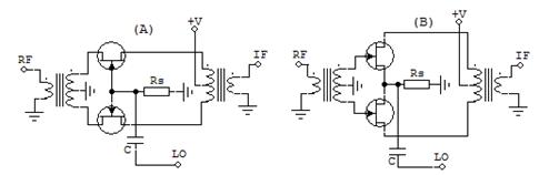
In order to optimize the complete balanced circuit was found that the configuration of the JFET transistors (common-gate or common-source) would make a difference in terms of its noise factor (noise figure), conversion gain, and intermodulation characteristics.
Active JFET Mixer Types: (A) Common-Gate, (B) Common-Source
The noise factor, and hence, receiver sensitivity of the common-gate mixer configuration was found to be 6dB worse than the common-source mixer configuration.
But the large signal handling capability (IP3) of the common-gate mixer is 6dB better than that of the common-source mixer.
In a balanced JFET mixer common-source configuration (as the one used in the presented receiver), frequency dependent terminations are needed at the mixer ports to maximize receiver sensitivity (lower noise factor), to maximize the conversion gain, to protect the circuit from large out-of-band signals, and to minimize the intermodulation (IM) distortion.
Desensitization in a receiver can be caused by LO spurious signals (and phase noise), which can allow strong nearby carriers to rise the receiver noise floor.
For a balanced mixer perhaps the most significant improvement compared to single-ended configuration, is the cancellation of the noise from the local oscillator port (LO), which includes noise at the RF, noise at the IF, and noise at Image Frequencies.
This cancellation makes it unnecessary to add high-pass and low-pass filters at the LO port.
However, IF power is still present at the RF port (due to limited IF to RF isolation). This can be minimized by using a LPF at RF input that “shorts” the image frequencies (Image Reject Filter). The result of doing this will be the best possible mixer conversion gain.
The intermodulation (IM) degradation in mixers happens mainly due to feeding back the 2nd harmonic of the RF input signal.
So, to improve intermodulation response of the mixer, the IF port also need a frequency dependent termination.
The mixers used in the receiver presented here use tuned circuits at the IF ports. Those IF resonant circuits provide a short at the harmonics of the RF input signal.
The LO signal must not drive the mixer’s JFET devices too far into cut-off, or the full conversion gain will not be realized.
Clipping or cutting-off the local oscillator waveform reduces the power at its fundamental frequency and, therefore, reduces the conversion gain. In addition, clipping shifts the bias point of the device causing a decrease in input impedance.
Using a balanced transformer for a differential injection of the local oscillator into the mixer, minimize the even harmonics of the oscillator, and hence, also minimizing their mixing products.
Placing the first IF filter (roofing filter) directly after the first mixer, however, eliminates the effects of out-off-band signals on the IF amplifier and following stages, and, at least for the intermodulation measure of the dynamic range, reduces the required range of the following stages by the amount in decibels of the selective attenuation of out-of-band signals.
Most of the HF receivers use high frequency for their first-IF (45 MHz up to 73 MHz), and the main reason of doing this it’s to place far away the image frequency, and making easier its rejection.
But if the topology of the super-heterodyne receiver use high-side LO injection (fLO > fRF) the image frequency (fimage) is always placed above the RF signal, and far enough to be rejected using simple (and cheap) low-pass filters.
fimage = fRF + 2*fIF if fLO > fRF
fimage = fRF - 2*fIF if fRF > fLO
In this case the first-IF can be implemented at lower frequency (9 MHz or 10.7 MHz). At those frequencies there is much easier to find good quality (and cheap) crystal filters.
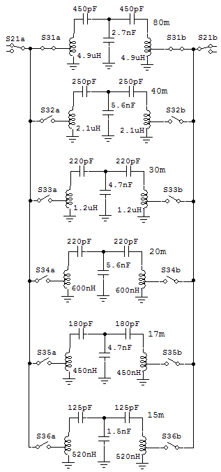
In the receiver presented below I used 10.7 MHz for the first-IF, and the working bands of the radio are: 80m, 40m, 30m, 20m, 17m, and 15m.
In the next table can see the relation between received frequencies (fRF), VFO frequencies (fLO), and image frequencies (fimage), when an intermediate frequency of 10.7 MHz is used:
|
Band |
fRF (MHz) |
fLO (MHz) |
fimage (MHz) |
|
80m |
3.500 |
14.200 |
24.900 |
|
40m |
7.000 |
17.700 |
28.400 |
|
30m |
10.100 |
20.800 |
31.500 |
|
20m |
14.000 |
24.700 |
35.400 |
|
17m |
18.068 |
28.768 |
39.468 |
|
15m |
21.000 |
31.700 |
42.400 |
The table above shows that using a steep low-pass filter in front of the first mixer (cut-off at 22 MHz), all the image frequencies (and afferent image noise) can be rejected.
Due to image noise foldover in a heterodyne receiver, removing the image noise can improve the receiver sensitivity up to 3dB. As a rule of thumb to get this benefit is necessary to have at least 20dB image rejection.
In our situation, the only disadvantage of this approach is that the receiver cannot be used for frequencies above 22 MHz (bands 13m and 10m). To receive those bands the low-pass filter must be removed.
For less than $20 you can build a DDS VFO with direct frequency reading based on AD9850 chipset, if you buy the components from here: DDS module, Arduino Nano module, LCD Display, Rotary Encoder.
The schematic of the DDS VFO, code and libraries, and any other information you can get from AD7C website. This useful DDS VFO have the ability to combine the VFO and IF frequencies and to show on the LCD display exactly the received RF frequency.
Another option for VFO circuit, is to use a PLL synthesizer using a Si5351 module, an Arduino Nano board, a Rotary Encoder, and an LCD display. The Si5351 module can get from here. PLL synthesizer is a better option than using a DDS, due to much lower inband spur emissions. The PLL synthesizer design could be based on the AK2B project. On the Internet are many other examples how to use the Si5351 module.
Generally, the noise performance of bipolar transistors is similar to JFET transistors.
In most situations JFETs are preferred because they have lower noise figure when higher impedances are used (case of resonant circuits in radio design) and also they exhibit low noise when high drain current is used, when BJTs have the lowest noise figure at low collector DC current.
An advantage using JFETs is that they can be placed in parallel. In this case the combined circuit provides higher gain and higher IP3 performance (due to greater power handling).
Interesting, in parallel placement configuration also the noise figure of the circuit is getting lower, due to increasing gain of the structure.
With the receiver presented, when the IF bandwidth is narrowed down to 1.9 kHz (using IF-shift) a noise floor of -140dBm can be obtained, for an SNR=10dB which is fine for SSB reception.
In terms of linearity, the front-end balanced LNA, using four J310 JFETs (Q1..Q4), have an IP3=+32dBm when is supplied at +20V, with a noise figure of about 0.5dB, and gain about 15dB.
The first mixer (Q5..Q8) have an IP3=+28dBm for an LO injection level of +7dBm and +20V supply voltage. Mixer gain is about 12dB and its noise figure is less than 3dB.
For the LNA I found that a quiescent current of about 9mA on each JFET transistor provides the best compromise for linearity and noise figure. For the mixer case the quiescent current should be slightly lower.
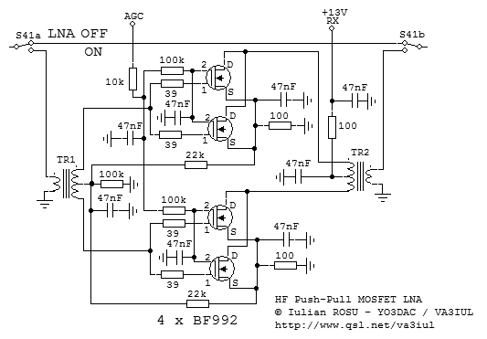
For the front-end LNA I have an option of a Push-Pull LNA controlled by AGC using four dual-gate MOSFETs (BF992, or any low noise dual-gate MOSFET as BF981, BF964, BF998, etc). The circuit provides even higher gain than the LNA using JFETs, but the IP3 is slightly lower, mainly due to lower supply voltage (dual-gate MOSFETs cannot be supplied at +20V as JFETs).
In all cases where common-source FETs were placed in parallel, a small value resistor was added in series to their gates to prevent any possible oscillations. Those resistors doesn't affect the noise figure of the amplifiers due to very high input impedance of the transistors.
On the receive side the radio use three IF frequencies (10.7 MHz, 455 kHz, and 97 kHz).
Good SSB filters for 10.7 MHz and for 455 kHz are easy to get. Also easy to get are the crystals for the down-conversion, 10.245 MHz and 358 kHz (NTSC sub-carrier crystal, 3.58 MHz divided by 10).
For the front-end Band Pass Filters I use T-type narrow band pass filters, with pass bandwidth equal exactly to the frequency range of each band. This approach, compared to usual BPF with 2 MHz bandwidth used by most of HF receivers, gives extra out-of-band rejection and lower insertion loss, and in this way lowering the in-band receiver noise floor. There are two topologies of the T-type BPF, first using top-capacitors and second using top-inductors. The top-capacitors topology gives better symmetry of the bandpass shape, but the top-inductor topology gives better out-of-band rejection at the high side of the filter (where the image frequencies are). Also the top-inductor topology its easier to be tuned. Needs to tune just the inductors value, when the top-capacitor BPF needs also to adjust (from band to band) the tap ratio of the inductors.
The 3rd IF of the receiver is on 97 kHz. This relative low intermediate frequency provides at the demodulated output an AF signal with a very high Signal-to-Noise Ratio.
Note that the 120kHz cut-off LPF used on the 3rd IF removes the wideband noise generated in the previous IF amplifiers and mixers, noise that would be generated in the last IF amplifier from the opposite side of the BFO, where it would otherwise be detected by the product detector as audio frequency noise.
The product detector is a double-balanced Schottky diode detector (BAR43S), which is kind of different than most of the similar product detectors, that usually are single-balanced. This provides an extra isolation of the output AF signal from the mixing products, and so, less distortions. The low noise audio signal is amplified first by a low noise audio preamplifier (Q19) and later by the TDA2030 audio power amplifier. Great attention was given to the audio power amplifier, because a lot of homebrew or professional receivers fails at this stage. TDA2030 which is a 12W audio power amplifier has very low distortions at 4W audio output (0.05%).
Special care must be given to the RX BFO working on 97 kHz (+/- 1.5 kHz). This is a free running LC oscillator, and good quality components is required to get the frequency stability. Stability which otherwise is not hard to be reached at this low frequency. Capacitors with (x) might need some tuning for adjusting the +/- 1.5 kHz carrier frequency shift.
The transmitter is pretty basic built, using a 10.7 MHz DSB modulator with SA612, and an SSB filter on 10.7 MHz which is used also by the receiver. The last stage TX MOSFET amplifier provides about 5W output in all desired bands.
RD06HHF1 and other RF power Mitsubishi MOSFETs you can get from here. The JFET J310 in TO-92 you can get from here, and in SMD package you can get from here. BF245C can replace J310 with some degradation of the intermodulation performances, due to lower IDSS. SA612 is available from here.
All "S" switches are low power Signal Relays which provides design simplicity, better intermodulation, better isolation, and lower insertion loss, than using switching diodes.
All the inductors, transformers, and capacitors should be measured with a digital LC-meter before placing them into the circuit .
For inductors and transformers I gave only the inductance values, because for a given inductance the number of turns varies significantly with the type of the ferrite used.
The capacitors part of the input HPF, BPF, and of the image reject LPF must have low tolerance values, to prevent increasing their in-band ripple.
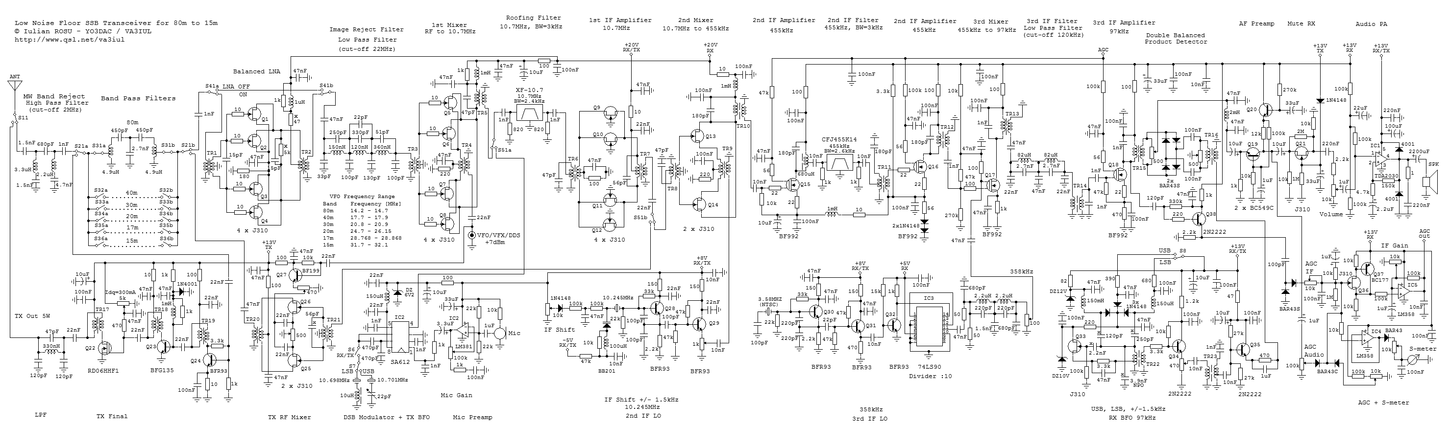
Schematic Diagram
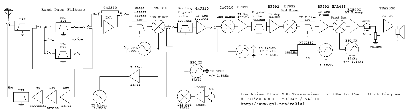
Block Diagram
Push-Pull MOSFET LNA controlled by AGC
|
Transformers Data |
Transformer Type |
|
|
TR 1 |
Prim.=1uH; Sec.=2 x 5uH |
Ferrite Toroid |
|
TR 2 |
Prim.=2 x 5uH; Sec.=1uH |
Ferrite Toroid |
|
TR 3 |
Prim.=1uH; Sec.=2 x 10uH |
Ferrite Toroid |
|
TR 4 |
3 x 3uH |
Ferrite Toroid |
|
TR 5 |
Prim.=4.7uH ; Sec.=470nH |
Ferrite Can IF |
|
TR 6 |
3 x 4.7uH : Prim. tap1/3 |
Ferrite Can IF |
|
TR 7 |
3 x 4.7uH |
Ferrite Can IF |
|
TR 8 |
3 x 4.7uH, Prim. tap 1/3 |
Ferrite Can IF |
|
TR 9 |
3 x 4.7uH |
Ferrite Can IF |
|
TR 10 |
Prim.=680uH ; Sec.=68uH |
Ferrite Can IF |
|
TR 11 |
Prim.=680uH tap 1/3; Sec.=68uH |
Ferrite Can IF |
|
TR 12 |
Prim.=680uH ; Sec.=68uH |
Ferrite Can IF |
|
TR 13 |
Prim.=2.7mH ; Sec.=270uH |
Ferrite Can IF |
|
TR 14 |
Prim.=270uH ; Sec.=2.7mH |
Ferrite Can IF |
|
TR 15 |
Prim.=2.7mH ; Sec.=600uH |
Ferrite Can IF |
|
TR 16 |
2 x 500uH |
Ferrite Can IF |
|
TR 17 |
2 x 5uH |
Ferrite Toroid |
|
TR 18 |
2 x 5uH |
Ferrite Toroid |
|
TR 19 |
2 x 5uH |
Ferrite Toroid |
|
TR 20 |
3 x 5uH |
Ferrite Toroid |
|
TR 21 |
3 x 1uH |
Ferrite Toroid |
|
TR 22 |
Prim.=430uH, tap 1/3; Sec.=50uH |
Ferrite Can IF |
|
TR 23 |
Prim.=270uH ; Sec.=2.7mH, tap 1/3 |
Ferrite Can IF |
Narrow Band Pass Filters
T-type BPF (top-capacitors) T-type BPF (top-inductors)