RF Power Meter
using for reading a standard Digital Voltmeter
Iulian Rosu, YO3DAC / VA3IUL, http://www.qsl.net/va3iul/

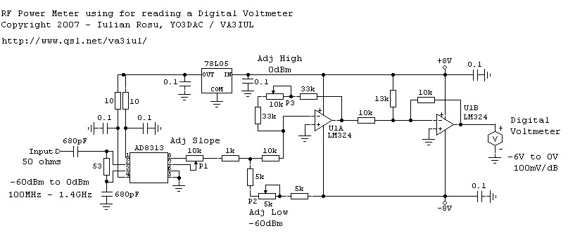
The RF Power Meter presented is based on the AD8313 Log Detector manufactured by Analog Devices.
The IC can be ordered as a sample direct from ADI (http://www.analog.com/en/), or you can search for it in some disabled GSM mobile phones available on the market.
In GSM phones AD8313 is used as a Log Detector, part of the Power Control Loop circuit. Generally could be easy identified near the Power Amplifier module.
AD8313 is a Logarithmic Detector which can accurately convert an RF signal at its input to an equivalent decibel-scaled value at its DC output.
The DC output is “linear in dB” with a basic slope of 20mV/dB. The slope can be adjusted in a range from 18mV/dB to 30mV/dB.
The linear input range of AD8313 is between -60dBm and 0dBm, which corresponds to a DC output between 0.6V to 1.6V (pin 8).
The following operational amplifiers (LM324) are translating the DC output range of AD8313 (0.6V to 1.6V on Pin nr 8) to a scaled range read by the Voltmeter (-6V to 0V). The scaled range has a resolution of 100mV/dB.
For example the minimum input value (-60dBm) corresponds to a read voltage value of -6.0V, -59dBm corresponds to -5.9V, -58dBm corresponds to -5.8V, and so on up to 0V that corresponds to 0dBm (as in the table below).
The frequency range of AD8313 is between 100MHz to 2.5GHz, but the range that not requires a dynamic slope adjustment is between 100MHz to 1.4GHz.
The resolution of the RF Power Meter is better than +/- 1dB; only near 0dBm power input, the resolution is approximately +/- 2dB.
The RF input has an impedance of 50 ohms provided by the 53 ohms resistor in parallel with the internal impedance of the AD8313.
For calibration inject first at the input an 800MHz signal at -60dBm and adjust P2 for -6V reading on the output Voltmeter.
After that increase the input level up to 0dBm and adjust P3 for 0V reading on the output Voltmeter.
The slope can be adjusted by the P1 semi-resistor.
Careful design of the RF input layout should be done for minimizing parasitics which can produce un-wanted resonances that affects the linearity vs frequency of the log-detector.
Tolerance of the resistors is +/-1%.
A calibrated attenuator at the input can be used to increase the maximum input power, without damaging the detector.
Correlation of the Input Power to the Output Voltage
| Input Power [dBm] | Output Voltage [V] |
| -60 | -6.0 |
| -59 | -5.9 |
| -58 | -5.8 |
| -57 | -5.7 |
| -56 | -5.6 |
| -55 | -5.5 |
| -54 | -5.4 |
| -53 | -5.3 |
| -52 | -5.2 |
| -51 | -5.1 |
| -50 | -5.0 |
| -49 | -4.9 |
| -48 | -4.8 |
| -47 | -4.7 |
| -46 | -4.6 |
| -45 | -4.5 |
| -44 | -4.4 |
| -43 | -4.3 |
| -42 | -4.2 |
| -41 | -4.1 |
| -40 | -4.0 |
| -39 | -3.9 |
| -38 | -3.8 |
| -37 | -3.7 |
| -36 | -3.6 |
| -35 | -3.5 |
| -34 | -3.4 |
| -33 | -3.3 |
| -32 | -3.2 |
| -31 | -3.1 |
| -30 | -3.0 |
| -29 | -2.9 |
| -28 | -2.8 |
| -27 | -2.7 |
| -26 | -2.6 |
| -25 | -2.5 |
| -24 | -2.4 |
| -23 | -2.3 |
| -22 | -2.2 |
| -21 | -2.1 |
| -20 | -2.0 |
| -19 | -1.9 |
| -18 | -1.8 |
| -17 | -1.7 |
| -16 | -1.6 |
| -15 | -1.5 |
| -14 | -1.4 |
| -13 | -1.3 |
| -12 | -1.2 |
| -11 | -1.1 |
| -10 | -1.0 |
| -9 | -0.9 |
| -8 | -0.8 |
| -7 | -0.7 |
| -6 | -0.6 |
| -5 | -0.5 |
| -4 | -0.4 |
| -3 | -0.3 |
| -2 | -0.2 |
| -1 | -0.1 |
| 0 | 0.0 |