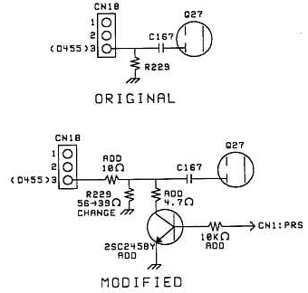

When the Processor-In control is set to some level below 10 dB of compression, a crackling noise can be induced on the transmit signal. The following modification will reduce the noise. After the modification has been performed, the noise can only be heard when the Processor-In control is set too low to be functional.
Note: This modification has already been performed on models starting with serial number 0120441.
Required parts:
Transistor (PNP)                      (2SC2458Y)
4.7 ohm, 1/6 watt resistor            (RD14CB2C4R7J)
10 ohm chip resistor                  (RK73FB2A100J)
39 ohm chip resistor                  (RK73FB2A390J)
10 Kohm chip resistor                 (RK73FB2A103J)
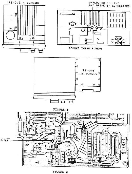
The following will be performed on the foil side of the Signal board.
This modification is covered under the 1 year warranty.
Time required to
perform the modification is 1 hour or less.
20-04-2000 TS-950SD N.B. Gate switching
noise
Author: Trio-Kenwood
Communication, inc.
Switching noise from the main band noise blanker circuit may be induced on the 15V line and pass through the AF amplifier to the speaker. The following modification will correct this condition.
Note: This modification has already been performed on models starting with serial number 104xxxx.
Required parts:
120 ohm, 1/8 watt resistor             (RD14BB2B121J)
100 µF, 16 V electrolytic capacitor    (CE04EW1C101M)
This work will be done on the component side of the AF board.
This modification is covered under the 1 year warranty.
Time required to
perform the modification is ½ hour.
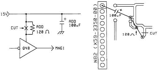
20-04-2000 TS-950SD Early protection with
TL-922A
Author: Trio-Kenwood
Communication, inc.
The TS-950SD RX to TX switching time in semi break-in is approximately 10 mS. At the key down, the transceiver momentarily sees an open circuit because the linear's keying relay has not engaged. As a result, the transceiver's protection circuit turns on, causing the output power to be reduced. The following modification will make the RX to RX switching time, in semi-break-in, approximately 30 mS. This modification does not affect full break-in switching. Increasing the switching time to 30 mS may restrict certain long distance high speed communications.
Required parts:
Digital transistor (QTY 2)                     (DTC124ES)
100 Kohm, ¼ resistor                           (RD14BB2E104J)
2.2 µF, 50 V electrolytic capacitor            (CE04EW1H2R2M)
This modification is covered under the 1 year warranty.
Time required to
perform the modification is 1 hour or less.
20-04-2000 TS-950SD RX digital
noise
Author: Trio-Kenwood
Communication, inc.
Some early TS-950SD transceivers may exhibit a low Signal to Noise ratio on ten and fifteen meters. In addition, rotating the encoder may allow the user to hear a crackling noise in his headphones. The following modification will correct this condition.
Note: This modification has already been performed on model from serial number 101xxxx.
This modification is covered under the 1 year warranty.
Time required to
perform the modification is 1 hour or less.
20-04-2000 TS-950SD Two second TX power
delay with MONI on
Author:
Trio-Kenwood Communication, inc.
When the MONI switch is turned on, transmit power may not develop for two seconds after key down. During this time, the ALC meter will pin and the SWR meter will read high. This will more likely develop on 18 MHz and 21 MHz bands. The following modification will correct this condition.
Note: This modification has already been performed on model from serial number 0120441.
Required parts:
2.2 Kohm chip resistor (RK73FB2A222J)
This modification is covered under the 1 year warranty.
Time required to
perform the modification is 1 hour or less.
20-04-2000 TS-950/SD Receiver
noise
Author: Trio-Kenwood
Communication, inc.
About 1 mV noise is present at the speaker or headphone jack in the receive mode with the AF GAIN control set to minimum. If the transceiver is in the CW mode, a faint tone might also be heard through the headphones (sidetone leakage). The following modification will reduce the level of the noise and the tone.
Required parts:
2SD1257K(S)
This modification may be covered under warranty.
Time required to perform
the modification is 1 hour or less.
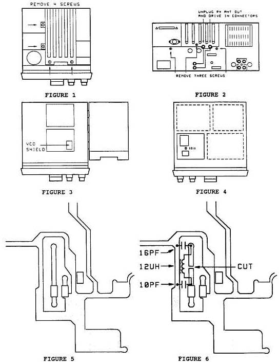
21-04-2000 TS-950S/SD TX image on 18.115
MHz
Author: Kenwood
Communication, inc.
Some TS-950SD owners have reported a transmit image at 18.115 MHz that cause the receiving station to hear distortion on the carrier. If the operating frequency is shift 3 KHz above or below 18.115 MHz, the image disappears. This modification will lower the image level from -30 dB (worse case) to better then - 40 dB by installing a trap on the 455 KHz I.F.
Required parts:
4 pF Trimmer capacitor              C05-0308-05
40 pF Trimmer capacitor             C05-0309-05
2.2 µH coil                         L40-2292-14
Modification:
Alignment:
This modification may be covered under 1 year warranty.
Time required to
perform this modification is 1 hour or less.
21-04-2000 TS-950S/SD 80 meter spurious
emission
Author: Kenwood
Communication, inc.
Some TS-950S/SD owners have reported a transmit spurious emission between 3.500 MHz and 3.520 MHz. The modification will reduce the spurious emission to - 65 dB.
Required parts:
10 pF capacitor           CC73FCH1H100J     QTY. 1
16 pF capacitor           CC73FCH1H160J     QTY. 1
12 µH coil                L40-1201-17       QTY. 1
2.6 X 4 mm screws         N09-0650-05       QTY. 4
This modification is covered under the 1 year warranty.
Time required to
perform this modification is 1 hour or less.
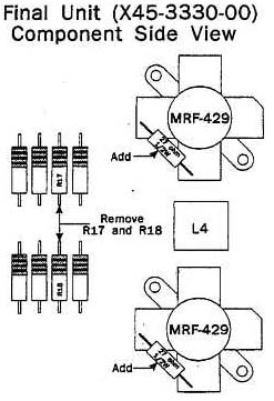
21-04-2000 TS-950S Final bias circuit
change
Author: Kenwood
Communication, inc.
It is possible to exceed the maximum Vcbo rating of the MRF429 transistors used in the TS-950S/SD if the unit is operated at excessive transmit power levels (greater then the normal factory output power setting). This results in a collector to base short on the MRF429. This causes excessive current to be drawn thru R17 and or R18 of the final bias circuit. This can cause a large amount of smoke from the overloaded resistors. It does not normally cause damage to surrounding components. (You might wish to check Q7, VR2, Q8 and the fuse just as a precaution!)
R17 and R18 are carbon type resistors (27 ohms ½ w). Carbon resistors can emit quite a bit of smoke when overload in this manner and can be the cause of considerable concern by the operator!
In order to case operator concern we recommend replacing R17, and R18 on the final unit (X45-3330-00) with ceramic resistors whenever replacing the final transistors. These special resistors have been designed to open quickly if the current rating is exceeded. This prevents smoking and the odors associated with burning resistors.
Parts required:
27 ohm ½ watt ceramic resistor, (R92-1286-05)
Precautions:
Replacement Procedure:
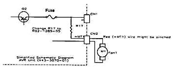
The 50 watt power down circuit will begin to operate if the cooling fan on the rear panel fails to operate after 15 minutes of continuous transmission in order to protect the final amplifier circuit. Failure of the fan will prevent the power down circuit from returning transmit power to normal levels since the transformer temperature remains high. This trouble can sometimes be traced to a pinched/burnt wire near resistor R17 of the AVR unit (X43-3070-01).
Causes:
If the red wire attached to the connector CN2 of the AVR unit is pinched between the chassis and ground the insulation might be damage and allow this line to be short to the chassis. This wire supplies 15 Vdc to the fan motor thru resistor R17. Excessive current is drawn thru R17 under this circumstance, approximately 1.5 A rather then the normal .5 A. This can cause the resistor to become red hot and damage the surrounding circuit board, since R17 is a metal oxide film resistor.
Corrective action:
R17 should be replaced with a ceramic resistor if this symptom is encountered. Replacing the metal oxide film resistor with a ceramic resistor will prevent damage to the circuit board should the red lead become shorted.
Parts required:
10 ohm 2 watt ceramic resistor, R92-1285-05
Occasionally the TS-950SDX will transmit instantaneously when the mode is switched from SSB to CW with the VOX turned on. The frequency of occurrance depends upon the setting of the VOX GAIN and DELAY controls.
Cause:
A small amount of RF feedback is felt on analog switches IC5 and IC6 in the AF unit. This RF causes the timing circuit to actuate briefly when the mode is changed with VOX ON.
Warning: This radio uses micro-sized surface mount component, and/or multi-layer circuit boards. If you are not familiar with the techniques for service of this type of equipment do not attempt this modification yourself. You will invalidate your warranty if you attempt to modify the equipment and damage the radio. If you are at all in doubt about your qualification to perform this modification you should seek qualified assistance.
Required parts:
C191: 4.7 µF, 25 V electrolytic capacitor (CW04EW1W4R7M)
Procedure:
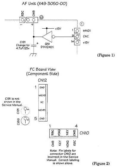
This modification may be covered under warranty.
Time required for this
modification is 1 hour or less.
22-04-2000 TS-950SDX No beep in
headphones
Author: Kenwood
Communication, inc.
Several owners of the TS-950SDX have reported the absence of an audio confirmation tone when using monaural headphones. The tone is present when listening with stereo headphones but only from the right hand speaker element.
Cause:
In this design the SUB AF PA circuit supplies audio when using a monaural headphone, and the MAIN AF PA supplies audio to the right speaker of a stereo headphone. The audio confirmation tone is not applied to both the SUB AP PA and the MAIN AF PA. To simplify circuit design the tone is only routed to the MAIN AF PA. Unfortunately this left monaural users without a confirmation tone and stereo headphone users with a confirmation tone only in the right side of the headphones.
Correct action:
The following modification permits the user to hear
the audio confirmation tone from both sides of a stereo headphone and from a
monaural headphone.
Warning: This radio uses micro-sized surface mount component, and/or multi-layer circuit boards. If you are not familiar with the techniques for service of this type of equipment do not attempt this modification yourself. You will invalidate your warranty if you attempt to modify the equipment and damage the radio. If you are at all in doubt about your qualification to perform this modification you should seek qualified assistance.
Required parts:
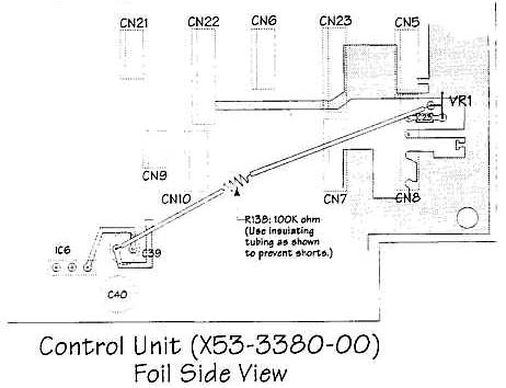
R138: 100 Kohm radial lead ¼ watt resistor, (RD14BB2C104J)
Procedure:
This modification may be covered under warranty.
Time required for this
modification is 1 hour or less.
22-04-2000 TS-950SDX Distorted DRU-2 TX
audio
Author: Kenwood
Communication, inc.
We have received several reports of minor distortion of the DRU-2 transmitted audio when used with the TS-950SDX. Recordings made from incoming received sources do not appear to be distorted.
Cause: This characteristic is caused by an impedance mismatch between the DRU-2 output and the input of the microphone amplifier circuit in the TS-950SDX. The following modification will correct/improve this characteristic.
Procedure:
On the Microphone Amplifier Unit (X59-3710-01), which is
part of Switch Unit (A) (A41-3240-00) (H/10): (The Microphone Amplifier Unit is
a small daughter board located on the switch assembly that has the Microphone
Gain/Power Output Control and the Speech Processor IN/OUT controls).
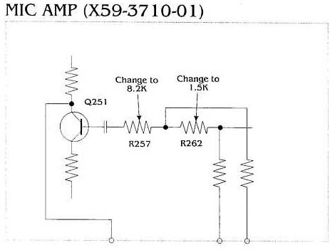
Time required for this modification is 30 minutes or less.
22-04-2000 TS-950SDX w/K1EA Ver. 8 Program
(Revised)
Author: Kenwood
Communication, inc.
We have received several reports of the transmitter unkeying when using the K1EA Contesting program. This symptom only occurs when the TS-950SDX is used with version 8 of the K1EA program. Apparently some of the more advanced control features of this new version of the program cause the radio to think the program has unkeying. A new EPROM is available that corrects this transmitter drop out.
Parts required:
IC-19 Microprocessor, (27C512RJDVF), QTY. 1
Procedure:
Caution: This modification requires soldering equipment rated for CMOS type circuits. It also requires familiarity with surface mount soldering techniques. If you do not have the proper equipment or knowledge do not attempt this modification yourself. Seek qualified assistance.
Time required for this modification is 30 minutes or
less.
22-04-2000 TS-950SDX Speech
processor
Author: Kenwood
Communication, inc.
Symptom:
Reports of low COMP meter sensitivity, or noise on the
transmitted audio when using the speech processor is normally a result of
misadjustment of the PROC IN control. This control is very sensitive and is
difficult to adjust properly.
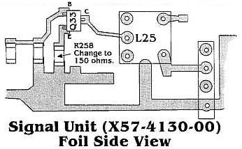
Parts required:
150 ohm chip resistor, (RK73FB2A151J)
Procedure:
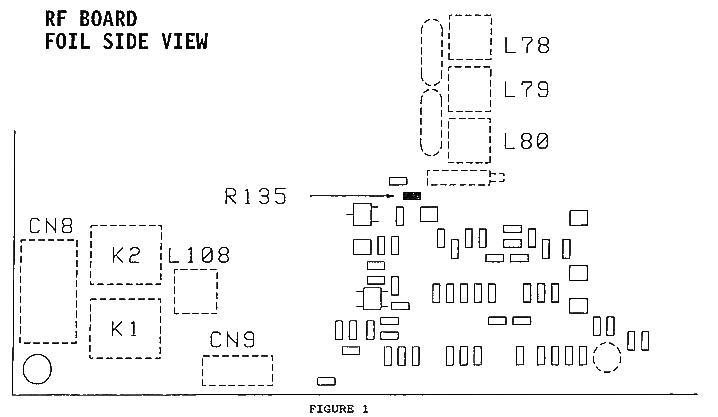
Change the value of R258 in the SIG unit (X57-4130-00)
from 68 ohm to 150 ohm. This will increase the available adjustment range of the
PROC IN control. This will make it much easier to properly adjust the control
and thus avoid overdriving the speech processor circuit.
Caution: This modification requires soldering equipment rated for CMOS type circuits. It also requires familiarity with surface mount soldering techniques. If you do not have the proper equipment or knowledge do not attempt this modification yourself. Seek qualified assistance.
Time required for this modification is 30 minutes or less.
22-04-2000 TS-950SDX 3rd order IMD
standardization
Author: Kenwood
Communication, inc.
Symptom:
3rd order IMD figures have been noted that do not meet out
standard value of -32 to -35 dB.
Cause:
We have found that this symptom can be caused by either
improper blas to the final transistor and/or because of distortion inducted by
the 73.05 MHz IF mixer circuit.
Parts required:
R195, R197, R198    150 ohm chip resistor   RK73FB2A151J     QTY. 3
R204                4.7 Kohm chip resistor  RK73FB2A472J     QTY. 1
R19, R20            22 ohm carbon resistor  RC05GF2H220J     QTY. 2
Procedure:
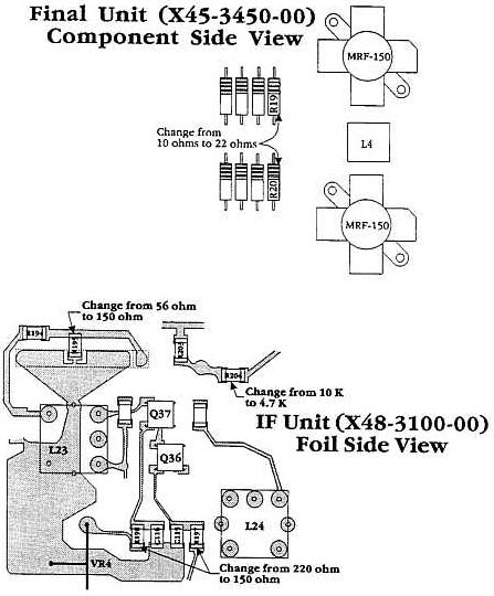
Caution: This modification requires soldering equipment rated for CMOS type circuits. It also requires familiarity with surface mount soldering techniques. If you do not have the proper equipment or knowledge do not attempt this modification yourself. Seek qualified assistance.
Time required for this modification is 1 hour or less.
22-04-2000 TS-950SDX Key click w/bug type
keyer
Author: Kenwood
Communication, inc.
Symptom:
A "bug" type keyer used at high keying speeds might cause
a key click or chattering noise on the transmitted signal. When the internal
electronic keyer is used no such chattering noise is encountered.
Cause: The internal chatter absorption filter circuit incorrectly tries to remove noise from the external keyer.
Procedure:
This operation turns off the internal chatter absorption filter circuit.
Time required for this modification is 15 minutes or less.
23-04-2000 TS-950 Hum with monitor
ON
Author: Kenwood
Communication, inc.
Symptom:
On early versions of the TS-950 series (below serial
number 106xxx) a hum might be heard when the MONI function is active and
headphones are connected to the PHONE jack. No hum is experienced when the MONI
circuit is OFF
Cause:
This noise can only be found in the monitor circuit itself
and not on the transmitted signal. We have found that the VCO shield cover for
the PLL unit might be contacting the shield plate for the filter unit. This
physical contact can allow a slight amount of vibration to be felt in the
sub-receiver section. This vibration, combined with too much gain in the
sub-receiver section contributes to the hum.
Parts required:
Qty    Description                          Kenwood Part No.    Circuit description
 4     Low profile PLL Unit cover screws    N35-2640-05         NA
Procedure:
Time required for this modification is 15 minutes or less.
23-04-2000 TS-950 Noise with Sub-Band noise
blanker ON
Author: Kenwood
Communication, inc.
Symptom:
Noise is generated when NB1 is switched on for the
sub-receiver.
Cause:
Switching noise from the noise-blanker gate enters the AF
amplifier via the +15 V line causing the noise.
Parts required:
Qty   Description                          Kenwood Part No.     Circuit description
 1    100 µF, 16 V electrolytic capacitor  CE04KW1C101M         NA
 1    120 ohm resistor                     RD14BB2B121J         NA
Procedure:
Time required for this modification is 15 minutes or less.
23-04-2000 TS-950 14.200 MHz transmit
spur
Author: Kenwood
Communication, inc.
Symptom:
A close-in transmit spur might be present on early model
TS-950(S) (serial number 1010xx and below) transceivers when operating at a dial
frequency of approximately 14.200 MHz. This spur is seen approximately -40 to
-50 dB down from the fundamental.
Cause:
The output from the mixer (IC12) which generates the final
PLL loop comparison frequency for the AF unit contains harmonic radiation at
approximately 36 to 68 MHz.
Parts required:
Qty   Description                          Kenwood Part No.  Circuit description
 1    Broad band transformer               L19-0346-05       L15
 1    .001 µF 50 V capacitor               CK45B1H103K       C127
Procedure:
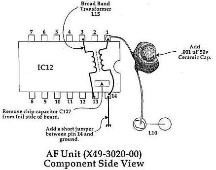
Caution: This modification requires soldering equipment rated for CMOS type circuits. It also requires familiarity with surface mount soldering techniques. If you do not have the proper equipment or knowledge do not attempt this modification yourself. Seek qualified assistance.
Time required for this modification is 30 minutes or less.
23-04-2000 TS-950 Low power output after
temp. protection
Author: Kenwood
Communication, inc.
Symptom:
After transmitting for approximately 2 hours at 50% duty
with 150 watts output the temperature protection circuit activates reducing the
output power to about 50 watts. Normally, full output power will be restored
after the fans have had a chance to cool things down. Occasionally the power
output will not return to normal, even after extended receive operations.
Cause:
The temperature sensor is attached to the main transformer
and is set to activate at 80°C. This setting was selected to reduce power before
the internal fuse on the transformer opens.
Correct action:
After through testing, we have found that the
temperature sensor should be set to 90°C to allow proper return to full power
transmit. This setting will also allow the radio to be used at higher ambient
room temperatures without worrying about the power output dropping in the middle
of a QSO.
Parts required:
Qty   Description                          Kenwood Part No.  Circuit description
 1    90°C Thermal switch                  S59-1416-05       S1
Caution: This modification requires soldering equipment rated for CMOS type circuits. It also requires familiarity with surface mount soldering techniques. If you do not have the proper equipment or knowledge do not attempt this modification yourself. Seek qualified assistance.
Time required for this modification is 30 minutes or less.
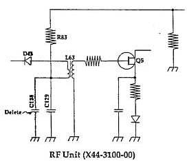
23-04-2000 TS-950 Infinite SWR at beginning
of transmission
Author: Kenwood
Communication, inc.
Symptom:
During "Full Break-in" operation the SWR meter shows
infinite SWR at the beginning of transmission. This results in a reduction of
the transmitter power, followed by a gradual increase to normal full power. This
symptom does not occur with the antenna tuner set to "THRU".
Cause:
Normally the RCB line should be 0 Vdc at the beginning of
transmit operations. We have found that this does not always occur. The length
of time required for transmit power to return to normally is directly related to
the time constant of capacitor C128 on the RXB line.
Correct action:
Removing this capacitor corrects the above symptom,
but might affect the receiver sensitivity at a dial frequency of 100 KHz. This
action is only recommended if the symptom is actually present. Do not modify the
unit if the symptom is absent.
 |
Caution: This modification requires soldering equipment rated for CMOS type circuits. It also requires familiarity with surface mount soldering techniques. If you do not have the proper equipment or knowledge do not attempt this modification yourself. Seek qualified assistance. |
Symptom:
When tuning into an antenna with high SWR the SWR meter
reading becomes unstable and a small amount of smoke is seen coming from the
antenna tuner.
Cause:
One of the 3 x 4 self tapping screws that is used to secure
the AT unit hinge can occasionally damage the insulation on the brown lead wire.
When the tuner is then load into a high SWR the high reflected voltage causes
the lead to head up, which further damages the insulation. Eventually the
insulation breaks down completely and the wire shorts to the screw causing the
lead to overheat and smoke to emanate from the area.
Correct action:
Cut a 12 cm long piece of the fiberglass insulating
sleeve and install it over the brown lead wire to prevent shorting.
Parts required:
Qty Description Kenwood Part No. Circuit description 12 cm Fiberglass insulating sleeve 212-3502-05 W101(Note: The insulating sleeve must be ordered in increments of 1 meter or greater).
Time required for this modification is 30 minutes or less.
23-04-2000 TS-950S/SDX Transmit
spur
Author: Kenwood
Communication, inc.
Symptom:
A transmitter spur might be present at a dial frequency of
xx.xx1 MHz. This spur (fo +/- 1 KHz) is quite small (-55 dB relative to fo) but
might become noticeable when the transceiver is used with a linear amplifier.
Cause:
The transmitted signal enters pin 5 of IC11 which is in the
last PLL loop in the AF unit due to RF feedback. This pin is the input for the
10 MHz Ref. Osc. signal from the CAR unit. IC11 is the source of the spurious
signal since both the band and 10 MHz frequencies are divided by the 500 KHz
comparison frequency supplies by IC11.
Correct action: To reduce this RF feedback increase the Ref. Osc. level from .2 V to .7 V ms by adding the accompanying circuit to the input of IC11.
Parts required:
Qty   Description                          Kenwood Part No.  Circuit description
 1    12 µH Ferri-inductor                 L40-1201-17       NA
 1    10 pF Chip capacitor                 CC73FCH1H100J     NA
 1    16 pF Chip capacitor                 CC73FCH1H160J     NA
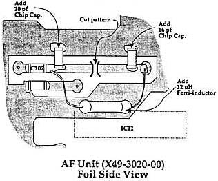
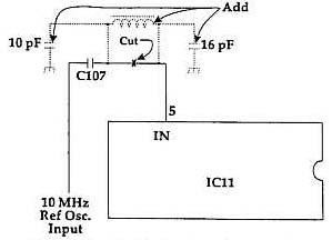
Caution: This modification requires soldering equipment rated for CMOS type circuits. It also requires familiarity with surface mount soldering techniques. If you do not have the proper equipment or knowledge do not attempt this modification yourself. Seek qualified assistance.
Time required for this modification is 30 minutes or less.
23-04-2000 TS-950SDX "click noise" with
NOTCH ON
Author: Kenwood
Communication, inc.
Symptom:
A click noise might be generated when receiving a strong
signal (S-0 or above) when the NOTCH is ON and the Notch Control is turned away
from the notch point.
Corrective action:
Lengthening the AGC release time of the IF Amp
just before the NOTCH circuits will correct this symptom. The enclosed
modification has been designed to change the time constant only when the NOTCH
circuit is activated. Do not install this modification on sets that do not
exhibit this symptom as the AGC FAST time constant affected by this change.
Parts required:
Qty   Description                          Kenwood Part No.  Circuit description
 1    0.047 µF capacitor                   CK45B1H473Z       NA
 1    Digital transistor                   DTC124ES          NA
 1    47 Kohm chip resistor                RK73FB2A473J      NA
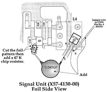
Caution: This modification requires soldering equipment rated for CMOS type circuits. It also requires familiarity with surface mount soldering techniques. If you do not have the proper equipment or knowledge do not attempt this modification yourself. Seek qualified assistance.
Time required for this modification is 30 minutes or less.
23-04-2000 TS-950SDX YG-455S-1 Installation
note
Author: Kenwood
Communication, inc.
Symptom:
When the YG-455S-1 is installed, the LSB audio is slightly
off pitch. This characteristic is corrected using the "Service Adjustment" menu.
Early models of this transceiver did not make this adjustment available the
individual operator unless they had access to a service manual.
Countermeasures:
A menu option has been added to Menu 07 on late
versions of the transceiver which allows the individual operator to "correct"
this audio shift. This has been accomplished by changing the program of the ROM
chip IC-19 on the Digital unit X46-3130 1/2, and by updating the operators
manuals. Installing the new ROM on early versions of this transceiver will allow
the operator the same convenience as provided on later serial numbered sets.
Parts required:
Qty   Description           Old part No.      New Part No    Circuit Description
 1    ROM                   27C512BJDUF       27C512BJDUG    IC-19
                                or
 1    ROM                   27C512RJDVF       27C512BJDUG    IC-19
 1    Instruction manual    B62-0229-30       B62-0229-40
Time required for this modification is 30 minutes or less.
23-04-2000 TS-950SDX No VFO B after
"split"
Author: Kenwood
Communication, inc.
Symptom:
Using the following key sequence will result in a failure
to receive on VFO B.
Countermeasure:
Press the 8.83 MHz FILTER select key one time, or
replace the ROM chip.
Parts required:
Qty   Description              Old part No.   New Part No    Circuit Description
 1    ROM                      27C512BJDUG    27C512BJDUJ    IC-19
                                   or
 1    ROM                      27C512BJDVG    27C512RJDVJ    IC-19
Time required for this modification is 30 minutes or less.
23-04-2000 TS-950SDX Carrier point
adjustment
Author: Kenwood
Communication, inc.
Symptom:
The background audio tone is different between the LSB and
the USB mode, when no signal is present, i.e. the carrier point is incorrect.
Occasionally, this tone is still different after adjustment per the service
manual, specifically Item 9 on page 196.
Countermeasure:
Change the adjustment procedure for Item 9 as
follows:
Test Equipment
Preparation:
Adjustment Procedure:
Time required for this modification is 60 minutes or less.
23-04-2000 TS-950SDX Sub band residual
noise
Author: Kenwood
Communication, inc.
Symptom:
The level of residual noise (AF VOL at Min) on the SUB
band is slightly higher than that of the MAIN band. This is especially true at
audio frequencies of around 50 Hz, as viewed on a spectrum analyzer. As a result
the SUB receiver is more susceptable to motor noise, such as might be generated
by fans, refrigerators, etc.
Countermeasure: Replacing the Control unit electrolytic capacitors (C33, C34, and C39) with Tantalum capacitors, and adding the bypass capacitor to the Switch unit reduces or eliminates this symptom.
Parts required:
Qty   Description                          Kenwood Part No.  Circuit Description
 1    0.1 µF 35 V Tantalum capacitor       C92-0001-05       C33
 1    1.0 µF 16 V Tantalum capacitor       C92-0004-05       C34
 1    10 µF 16 V Tantalum capacitor        C92-0505-05       C39
 1    .01 µ disc capacitor                 CK45B1H103Z       NA
Caution: This modification requires soldering equipment rated for CMOS type circuits. It also requires familiarity with surface mount soldering techniques. If you do not have the proper equipment or knowledge do not attempt this modification yourself. Seek qualified assistance from your closest Kenwood Service Center (Long Beach, CA, or Virginia Beach, VA).
Time required for this modification is 60 minutes or less.
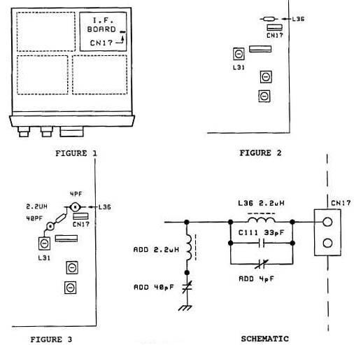
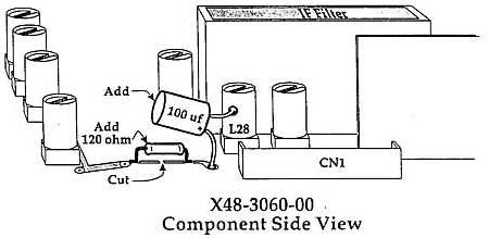
23-04-2000 TS-950SD 18.115 MHz
spur
Author: Kenwood
Communication, inc.
Symptom:
Transmitting on 18.1145 MHz causes a spur to appear at
18.1150 MHz with the antenna tuner on.
Corrective Action: Add the low pass filter shown in the accompanying diagram to the input circuit of mixer Q41 on the IF unit (X48-3060-00). This filter will increase the attenuation by approximately 20 dB.
Parts required:
Qty   Description                          New Part No.      Circuit Description
 1    220 µH inductor                      L40-2211-14       NA
 1    220 pF chip capacitor                CC73FSL1H221J     NA
Caution: This modification requires soldering equipment rated for CMOS type circuits. It also requires familiarity with surface mount soldering techniques. If you do not have the proper equipment or knowledge do not attempt this modification yourself. Seek qualified assistance from your closest Kenwood Service Center (Long Beach, CA, or Virginia Beach, VA).
Time required for this modification is 60 minutes or less.
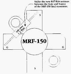
23-04-2000 TS-950SDX Change of Gate resistor
type
Author: Kenwood
Communication, inc.
Symptom:
If the final amplifier is operated at excessive transmit
levels (over 150 watts output) the final FET's may fail and short from Source to
Gate. If this occurs, the bias resistors used in this circuit may be damaged and
cause a large amount of smoke to be emitted from the final compartment.
Corrective Action:
Change the carbon type resistor used for R17 and
R18 to the fuse type resistors specified below. This will prevent an unpleasant
odor and smoke from the final compartment.
Parts required:
Qty   Description                          New Part No.      Circuit Description
 2    100 ohm ½ watt fuse resistors        R92-1310-05       R17, R18
Procedure:
Caution: This modification requires soldering equipment rated for CMOS type circuits. It also requires familiarity with surface mount soldering techniques. If you do not have the proper equipment or knowledge do not attempt this modification yourself. Seek qualified assistance from your closest Kenwood Service Center (Long Beach, CA, or Virginia Beach, VA).
Time required for this modification is 60 minutes or less.