From: abe riazi ([email protected])
Date: Fri Dec 29 2000 - 10:10:37 PST
Dear Scholars:
A branch of "pre-route" simulation with growing importance is frequently referred to as "solution space exploration". A prime objective of this methodology is to determine the constraints (or design space) that offers maximum PCB layout flexibility.
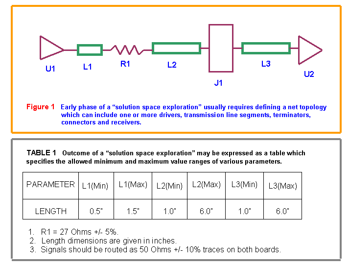
At an early stage of a design space exploration, it is customary to define a network topology (i.e. specific placement arrangement of the components, or element node to node interconnect) as illustrated by Figure 1, which can contain one or more drivers, transmission line segments, terminators, connectors, and receivers. These components in turn demand accurate models compatible with the simulator program. Furthermore, in order to produce reliable simulation results, package parasitics should be also included for each driver and receiver model.
Figure 1 may be viewed as a generic representation of a multi-board topology, such as a memory or PCI/PCIX bus commonly observed in a high speed design. For instance, when representing a memory bus, U1 can correspond to a chipset, L1 a stub length, and L2 a trace length on the motherboard. J1 would then be a memory connector, L3 length of a transmission line and U2 an IC on the (daughter) memory board. It should be noted that Figure 1 shows a unidirectional signal; however, the signals can be bi-directional in many cases. It should be emphasized that Figure 1 is meant to be only a simple example, having only one connector and a single add-in card; whereas, a net belonging to a complex bus may encompass multiple connectors and plug-ins.
Parametric sweeps and Monte Carlo (statistical) are among analyses normally carried out during a solution space exploration. A critical aim is to capture the best and worst case corners. During simulations, it may be necessary to modify termination schemes, add or remove components, change routing topologies, vary trace characteristics (i.e. length, impedance, velocity, etc.), or alter driver/receiver strength (or technology). Although, Monte Carlo can help to appraise the sensitivity and stability of system under design, sometimes a solution space is created solely based on sweeps (i.e. without aid of Monte Carlo).
Signal quality degradations (i.e. overshoot, undershoot, oscillation, ringback, etc), crosstalk effects, setup and hold timing violations, as well as mechanical (and thermal) considerations (which may influence PCB route-ability)are among criteria utilized when determining constraints. SI violations can be detected by visual waveform inspection and/or evaluation of the ASCII report files commonly generated by simulators. When ascertaining boundaries of the design space, it is helpful (and often necessary ) to create Excel spreadsheets and/or 3D surface plots utilizing results of parametric sweeps.
Table 1 illustrates a possible format for presenting outcome of a solution space analyses; though it shows only a simple type of results. More complicated versions can include additional restrictions such as length matching (for instance: | L2 - L3 | < 0.5 " ), aggregate length constraints (for example: 2.0" < (L1 + L2 + L3) < 10.0" ), or crosstalk rules (such as: signals must be separated by 4x the trace height to reduce crosstalk). The outputs of a solution space exploration are also frequently expressed as 2D or 3D graphs.
The minimum and maximum parameter limits of a design space are usually transferred as routing (DRC) constraints to a PCB routing program. Upon completion of layout, post-route simulation normally follows to verify the validity of pre-route rules and to ensure that the solution space constraints have been accurately transferred to the CAD program. This also indicates that the creation and verification of a solution space may require a very large amount of simulation runs.
To summarize, "solution (or design) space exploration" described is one type of "pre-route" simulations to ascertain workable and versatile PCB layout constraints. Some critical steps consist of defining a topology, obtaining models, performing simulation, collecting and analyzing waveforms (and SI data), and presenting results. During the course of simulation numerous physical parameters may be varied including trace lengths, impedance, velocity, termination style or values (within the tolerance range ), routing topologies, or driver technologies, etc. Parameter sweeps and targeted Monte Carlo analysis are two commonly employed simulation techniques; but the former appears to be more dominant (i.e. many solution spaces are generated by means of parameter sweeps only and without Monte Carlo). The outcome of solution space is normally presented as a table, spreadsheet, 2D or 3D graphs. After inputting the constraints to a PCB layout program and upon completion of routing (in accordance with constraints), it is recommended to follow up with post-route simulations in order to examine the validity of the results.
I like to genuinely thank you for your valuable comments and wish you all a wonderful holiday season and a prosperous New Year.
Abe Riazi
ServerWorks
2251 Lawson Lane
Santa Clara, CA 95054
**** To unsubscribe from si-list or si-list-digest: send e-mail to
[email protected]. In the BODY of message put: UNSUBSCRIBE
si-list or UNSUBSCRIBE si-list-digest, for more help, put HELP.
si-list archives are accessible at http://www.qsl.net/wb6tpu
****
This archive was generated by hypermail 2b29 : Tue May 08 2001 - 14:30:31 PDT