Switching Power Supplies for Tube Heaters
The switching power supply is a viable alternative to the conventional power transfromer
for supplying power tube heaters. A typical switcher will be lighter, perhaps smaller,
and provide better than 1% regulation over all reasonably expected line & load variations.
However, it is not practical to connect a "stock" supply directly to a tube heater.
The cold resistance of a heater is a fraction of the hot value and excessive current will flow on the
order of 3-4X the rated value. Even though this condition will persist for only a second or two,
it may be deleterious to both the switching supply and the (expensive!) tube.
Some older discreet component switchers may be modified for an extended turn on ramp.
Unfortunately, as switching supplies have become more integrated, it has become more difficult,
if not impractical, to modify their turn on characteristics to be suitable as heater supplies.
There is a simple external solution.
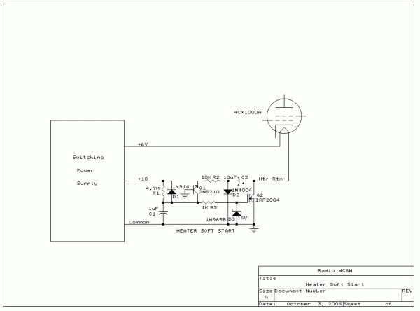
The circuit shown above provides a twenty second turn on ramp.
The power supply used was originally a 5 volt, +/-15 volt unit but, it had enough headroom
to output 6 volts which increased the tracking outputs by a corresponding percentage.
A brief operational description referring the circuit diagram above.
C2 is charged to the full heater potential at "power on" thru D2.
A slow ramp generated by R1, & C1, is applied to the gate of the power FET, Q2.
As the FET reaches its threshold voltage, circa 3 volts, the drain voltage
will begin to decrease which will delay the gate ramp by discharging C2
into the gate ramp, level shifted by Q1, a 2N5210 transistor.
This delays the ramp for approximately 18 seconds around the FET's threshold
and the heater current is thus limited to approximately its final value -- 10 amps.
The effective heater voltage rate of rise is 1/3 volt per second
R3, the 1K gate resistor precludes the power FET from oscillating and
D3, a 15 volt zener provides an upper limit to the ramp voltage.
The power FET employed has very low on resistance, circa 3 milli-ohms, when driven hard on.
During the power on ramp, the FET will dissipate about 30 watts max.
A small heatsink is advisable to avoid an unnecessary thermal excursion.
After the power on cycle completes, the FET will only dissipate a fraction of a watt
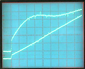
Observed with a current probe & storage 'scope, the heater current is actually seen
to decrease slightly, after the initial surge, as the heater's resistance increases
at a faster rate than the applied voltage.
The upper trace is the heater current -- 2 amps per division.
The lower trace is the heater voltage -- 1 volt per division.
The time base is 2 seconds per division.
The ramp completes just a skosh off screen right.
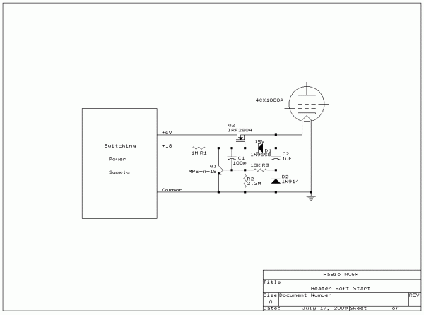
Here's a version with the Power FET in the positive lead, permitting direct grounding one side of the heater,
to accomodate those tubes which share a pin with the cathode. Operation is similar to the previous circuit.
R1 provides gate drive to the FET. Q1 is driven from the output, forcing the gate drive to ramp up
with timing set by C2, R2; as long as Q1 has enough gain such that it's base current is a small.
fraction of the current through R2. D2 provides a path to quickly discharge C2 at power down.
Incidently, a single output switching supply may easily modified for use in this application.
A voltage doubler may be connected (internally) at the secondary of the output transformer
to generate the required bias voltage (18-24 volts) for the FET.
Since the bias need only supply 25 uA, the doubler components may be very small.
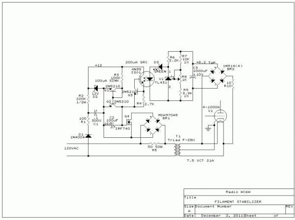
An AC Filament Stabilizer
Here's a thingy that I tinkered together out of curiousity a while ago.
It's a stabilizer rather than a regulator as it has necessarily slow response time.
It can only reduce the applied voltage so it may be necessary to provide a small boost transformer on the input.
No auxiliary power supply is required by this circuit.
R5 provides startup power to the circuit.
R10, BR2 & C3 provide the power for the secondary side circuitry and a peak detected value for the filament voltage.
R7, R8 & R9 sample the output voltage for U1 the regulator IC.
If the output voltage is too low, R6 & D3 provide source current to ISO1, the optoisolator.
If the output voltage is too high, this current is diverted through U1 and ISO1 receives no drive.
In actual operation there is about 20 mV of ripple on the peak detected filament voltage which results in a pulse width signal driving the optoisolator.
The output of the Optoisolator when active, in conjuction with Q4, sources 200 uA to the Power FET gate.
R3, Q1 & Q2 form a current mirror which continously sinks 100 uA from the Power FET gate.
C2 integrates the currents from the source & sink circuits.
The response of this circuit is slow enough that specific soft start circuitry is not required.
Q4, the Power FET in conjuction with BR1 provides a resistive attenuation of the AC input.
Note: I tried a dual (back to back) Power FET configuration in lieu of the bridge but, the mismatch between FET's was such that asymmetric transformer drive ensued.
Additional circuitry to balance the FET drives could be added though, the complication would be ... inelegant.
D1, D2, R1, R2 & C1 provide a 12 volt supply for the primary side circuitry.
The output voltage may be set by connecting a true RMS meter across the filament and adjusting R8 to the desired value. The peak voltage may not exactly track the RMS value but, over the limited range of operation it's close enough for Amateur Radio.
The circuit as shown is designed for 7.5 volt operation. Other voltages, and currents, could be accomodated with suitable component value adjustments.