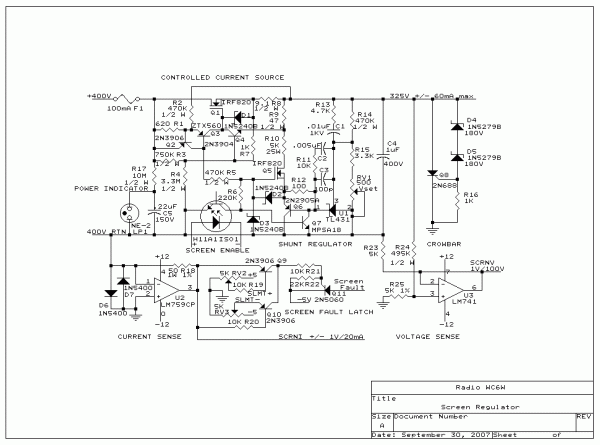
Screen Regulator
This is a floating shunt regulator with line/load regulation better than 1/2%
over its design current range.
No auxillary power supply is required for operation.
The system ground may also be connected to either the positive or negative line
to facilitate metering or a directly grounded screen configuation.
The regulator is comprised of a series current source plus a shunt voltage regulator.
The current source is limited at the maximum regulator output current.
Foldback limiting is also incorporated to limit the series element dissipation under overload conditions.
The shunt regulator incorporates a high wattage resistor in series with the control element
to reduce its average dissipation.
The shunt current additionally controls the series current source
so that only the current required by the load is supplied and if substantial negative current is introduced
via the output, the current source is clamped off to reduce the dissipation in the shunt regulator.
The values shown in the schematic below are selected for a 325 volt output at +/- 60 mA.
While the supply will function with as little as 10 volts of ceiling, a nominal 400V
unregulated source is specified to provide for low line operation.
Incidently, should the source voltage supply fail, the shunt portion of the regulator
will still function normally for negative screen currents.
This basic design may be extended to 1KV and several hundred milliamperes output
with upgrades in component types and some changes in part values.
Above 1KV, both the series and shunt FET's would have to be comprised of seriesed components.
Regulator Circuit Description
Controlled Current Source -- Q1, Q4, R8 and R9 comprise the series portion of the regulator.
R8 sets the maximum current output.
R9 sets the Controlled Current Source cutoff point during
negative Screen current excursions.
Q1 needs to be heatsinked for 10 watts
and rated for the full input voltage.
D1 provides gate protection to Q1.
Q2, Q3, R1, R2 and R5 fashion a nominal 1mA current source which provides gate bias to Q1.
R2 reduces the current through Q3, by sinking additional current through R1,
when the output is off, or shorted, to reduce the power dissipation in Q3.
Q3 must be rated for the full input voltage
Foldback Limiter -- R7, R3 & R4 bias Q4 to implement a foldback limit of the
Controlled Current Source.
Note that R3 & R4 are half watt devices for their voltage rating
not the power applied.
With the values shown, the limit is approximately 20mA into a dead short.
The ultimate limit current may be reduced at the expense of increased turn on time.
Shunt Regulator -- U1, Q6 & Q5 plus their associated components comprise the shunt regulator.
R10 sets the maximum negative current and dissipates a goodly portion of the shunt power.
Q5 need only be heatsinked for 10 watts and must be rated for the full input voltage.
D2 provides gate protection to Q5.
R5 and D3 bias Q5 for cascode operation.
Q6 and R12 form a current amplifier
between the output of U1 and Q5.
The output of U1 is limited to about 7 mA
to avoid unnecessarily heating the voltage reference and additional current
for the shunt path is provided via Q6 which is connected as an Emitter follower.
C2, C3 and R11 stabilize U1, an integrated circuit shunt regulator.
R14, R15 and RV1 form a voltage divider which sets the regulator reference voltage.
The divider is calculated to source 2.5V to pin 3 of U1 from the output.
C1 and R13 improve the dynamic response of the circuit which would otherwise
be somewhat poor given the large static feedback ratio.
C4, the output bypass capacitor may be increased without bound for greater stability.
Note that this will increase the turn on/turn off time.
Screen Enable circuit -- Q7 and R6 implement a "normally off" function.
Screen voltage is enabled by driving ISO1 which cuts off Q7 and enables the output.
With C4, the output capacitor shown, the turn on delay is 20 mS.
The "off" voltage output is circa 15V and the turn off delay is 10 mS.
Safety, Metering, and Overload Sensing Circuitry
for a negative ground application
Crowbar -- D4, D5, Q8 and R16 provide ultimate protection to the tube,
the socket bypass capacitor(s) and the regulator in the event of a regulator fault or flashover.
For best protection against a flashover, the crowbar circuit should be placed in close proximity
to the tube socket.
Fuse F1 protects the source supply against a catastrophic regulator failure.
A crowbar activation absent component failure will not blow this fuse.
HV Pilot Lamp -- R17, C5 and LP1 form a blinking neon indicator which warns that HV is present
at the input to the regulator for those of us who can't directly view high potential electrons.
Current Metering -- U2 and R18 sense the negative side of the Screen supply
and provide a 1V per 20 mA output for metering which may drive a center zero meter
with a +/- 5V movement and a +/- 100mA scale.
D6 and D7 protect U2 from arc overloads.
Overcurrent Sense R19, RV2 and Q9 set and sense the positive current overload point
triggering Q11 through R21.
R20, RV3 and Q10 function similarly for a negative currents.
Q11 may be connected to disable the screen supply and activate a warning indicator (not shown).
Voltage Sense -- R24 and R25 form a 100-1 divider which is buffered by U3
to drive a meter with a 5 volt intrinsic movement and a 500V scale.
R23 provides a current to the current metering circuit to cancel the drain of the voltage sense R's.
