At the moment, this document is just an unstructured collection of notes, started by DL4YHF 2017-01-15.
It will eventually make it into an additional 'hardware description',
besides the lots of details that you will find in the MD380 Tools already.
To microcontroller nuts like myself: Don't miss Travis Goodspeed's 'Reverse Engineering the Tytera MD380' at
www.qsl.net/kb9mwr/projects/dv/dmr/Reverse Engineering the Tytera MD380.pdf.
That article also contains a part of the circuit diagram. The complete schematics
are available online,
also some photos from the inside for the FCC registration.
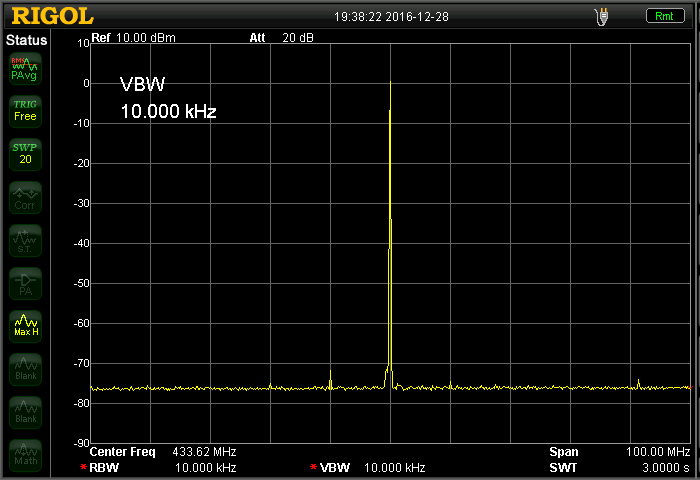
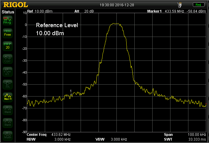
DMR transmit spectra measured before and hard- and software modification: Wideband spectrum (span = 100 MHz) Narrow band spectrum (span = 100 kHz)
Compared with some other low-cost handheld transceivers, the TX spectrum is remarkably clean.
Power consumption (measured directly at the battery terminals at 8 V):
With the original firmware, during idle, with backlight off: circa 70 mA
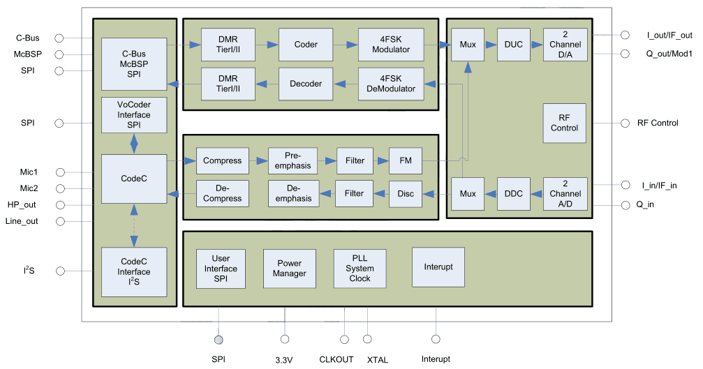
The datasheet for the HR_C5000 is mostly in Chinese. As Travis before,
I tried to let the 'big brother' translate some of the chapters..
results here. The chip's
block diagram on page 3 is quite informative:
Block diagram from the HR_C5000 datasheet
The HR_C5000 performs the DMR encoding (Tier I/II), contains an A/D converter
for the microphone, a D/A converter for the speaker, an I2S (digital audio)
interface to access the audio codec (note: that's not the vocoder).
The 'RF' (IF) ports use quadrature signals
for transmission and reception. It is designed to co-operate with an external
(!) 'VoCoder', connected via SPI (!). In this case, the vocoder is the CPU itself
(STM32F405). From the HR_C5000's point of view, the CPU 'looks like'
an AMBE-chip. For analog FM, there's a path from the audio codec to the modulator (FM TX),
and (for FM RX) a path from the FM discriminator to the codec, from codec to I2S,
and from I2S (pins I2S_FS → PA15, I2S_CK → PC10, I2S_TX →
PC12, I2S_RX → PC11) to the CPU (2016-12-27: beware, this wasn't verified yet).
The STM32F4 reference manual (RM0090) calls their equivalent 'SAI' (serial audio interface).
The STM32F405 datasheet ("DocID022152 Rev 8", page 56) tells us that...
- pin PA15 can be configured as 'I2S3_WS' ('word strobe' ~~ 'frame sync'),
- pin PC10 can be configured as 'I2S3_CK' (digital audio clock),
- pin PC12 can be configured as 'I2S3_SD' (serial audio data out),
- pin PC11 can be configured as 'I2S3ext_SD' (serial audio data in).
If more details about the control registers inside the HR_C5000 were known,
we could use the STM32F4 as a DSP (the CPU is powerful enough, as users of the
famous STM32F4xx-'discovery'-boards will confirm). Unfortunately there's
no obvious signal path between the DUC (digital up-converter), DDC (digital down-converter),
and the HR_C5000's audio codec (which would have to be a fast
stereo DAC for that purpose). If there was, we could play real 'software defined radio'
with this rig.
2.1 Audio signal paths in the RT3 / MD380 and the 'baseband' chip
The already mentioned MD380 schematics (MD-380UHF-RF-schematic.pdf) shows most, but not all details (and some
CPU connections are wrong). At least the analog signal paths are easy to follow,
and appeared to be correct.
It was a mystery to me how the CPU (STM32F405) 'knows' the position of the analog volume potentiometer.
In the schematics, the pot's wiper is only AC coupled. But instead (not shown in the schematics), it's also DC-coupled
through a low-pass filter to an analog input of the CPU. Carlos, EB4FBZ, described this at github.com/travisgoodspeed/md380tools/issues/98 .
The schematic diagram (from 'Peter', 2014-11-08) doesn't show the entire truth about the
signal path for message beeps: When 'Tones/Alerts' are enabled in the 'Radio Settings'
menu, they are audible in the speaker with a constant volume, regardless of the
analog potentiometer between 'VOL_OUT' and the speaker PA (U204).
But the schematic diagram only shows these audio-related outputs from the CPU:
STM32F405 PC8, 'BEEP' → 2nd order RC lowpass → ?? "VOL_OUT" → volume pot ?? → audio amp → speaker
STM32F405 PC8, 'BEEP' → 2nd order RC lowpass → "2T/5T/DTMF_OUT" (enters the HR_C5000, thus only for TX)
STM32F405 PC7 (no label) → another RC lowpass → "CTC/DCS_OUT" (modulates the transmitter, not for the speaker)
Guesswork: Another inacuracy in the schematics. More likely:
The low-pass filtered 'BEEP' is routed directly to the audio amplifier, bypassing the volume control pot.
A test with a rectangular wave (generated on PC8) confirmed that
such a signal path (bypassing the pot) exists.
To generate a tone locally for output to the speaker, ...
the audio power amplifier must be turned on by setting 'AFCO' (STM32 PB9) high,
some milliseconds later, the 'Anti-Pop' switching MOSFETS at the speaker output must be turned on
by setting 'SPK_C' (STM32 PB8) low,
PC8 must output PWM (square wave only, because PC8
cannot be configured as a D/A converter output)
The above findings were incorporated in isr_handlers.c (a contribution to the MD380-tools),
along with a simple Morse generator which was later used to announce the current channel name
for visually impaired hams.
For DTMF- and other signalling tones:
STM32F405 PC8, 'BEEP' → 2nd order RC lowpass → 2T/5T/DTMF_OUT' → HR_C5000 pin 5 'MIC2_P'
The signal paths inside the HR_C5000 from 'MIC_P1' (here: voice) and 'MIC_P2' (here: DMTF & Co) to the modulator (for FM),
or to the vocoder interface (for DMR), are quite complex. More on that in the list of registers,
translated from the chinese HR_C5000 datasheet. Some of the details were not fully understood at the time of this writing,
but experiments with the MD380 Tools (and the patched firmware) gradually shed more light on this.
With a modified variant of the md380-tools ( tool2.py with "c5write" to invoke c5000poke() via command line), various registers were modified
during transmission, in FM and DMR-simplex. This way, I tried to find out which of those registers (and bits)
really affect the signal path, and if / when those registers were overwritten by the remaining parts of the 'original' firmware. Conclusions:
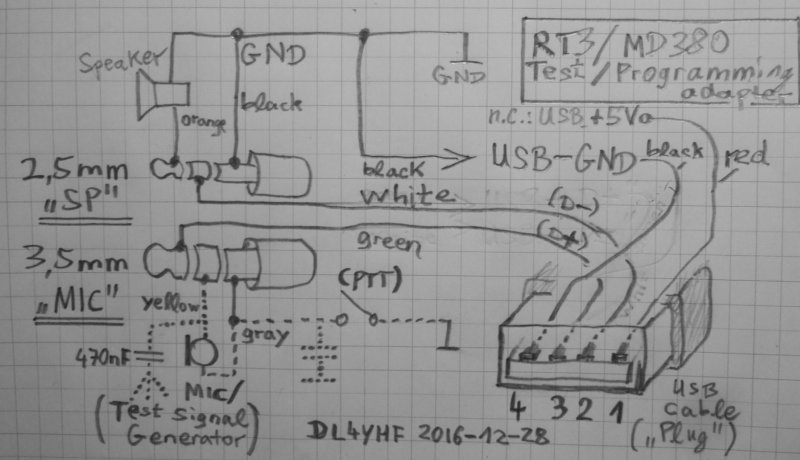
To test the MD380's 'microphone' path during transmission, by peeking and poking C5000 registers via USB,
you need a homemade adapter cable with the USB- and audio lines exposed
(because the radio mutes the internal microphone when plugging in the normal USB adapter cable)
While transmitting in FM, the modulation index of DTMF tones ("beeps") is affected by register 0x0F bits 7..3
The C5000's "Mic2" input was enabled while sending DTMF tones via bit 1 in register 0x0E ("Mic2En")
The C5000's "Mic1" input was enabled while sending FM-voice via bit 2 in register 0x0E ("Mic1En")
There are different, and slightly incompatible displays used in the RT3/RT8 and MD-380/MD-390.
The modified firmware (md380tools) makes a distinction of cases in applet/dispinit.c, based on information
read from a special area in the SPI Flash.
The display in the author's RT-3 was labelled 'HG01802008-B'.
It is connected to the CPU via an 8-bit port, with some signals configured as FSMC (static memory interface):
The framebuffer is in the display itself. The display controller is fairly compatible
with an ST7735 (the actual chip is an HX8302A, for which no sufficient datasheet was found yet).
The pin numbers shown for 'J101' above apply to the 24-pin flat ribbon cable
between main board and keyboard/display PCB.
Only when the display image is modified, there is 'activity' on this 8-bit interface between CPU and display.
Unfortunately, such a data transfer caused some radio interference that can even be picked up with another radio,
switched to SSB or FM, located near the RT3 / MD-380.
Obviously the manufacturer tried to reduce RFI emitting from the cable between CPU and display board
by connecting 1 kOhm series resistors in the eight data lines. Also, to make the 'display QRM' less apparent,
the firmware hides the display of the current time (and thus avoids periodic transfers) when the squelch is open in FM.
In attempt to read out the contents of the framebuffer, thin wires were attached
to LCD_RD, LCD_WR, LCD_RS, LCD_CS to check the timing with an oscilloscope.
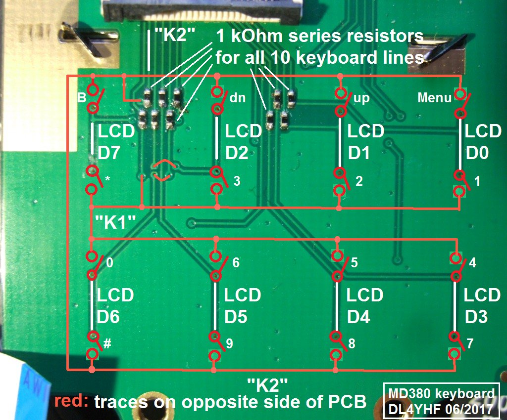
There are five 22-Ohm SMD resistors on the keyboard PCB where these
control signals can be tapped.
The keyboard consists of a matrix of rows and columns. Some of the keyboard signals
are shared with the LCD interface (see previous chapter). The original Tytera firmware
uses several of subroutines for the multiplexed polling, invoked from an extra task.
In the D13.020 firmware, these are called from 'kb_handler_sub1' at 0x0804F7DC (code
address). Shortly before returning, that function configures
the I/O ports to access the LCD again ('ConfigureLCDPort' at 0x08051F22).
     PA6  : multiplexer output, CPU to keyboard "K1", J101 (connector) pin 2
     PD2  : multiplexer output, CPU to keyboard "K2", J101 pin 3
     PD3  : multiplexer output, CPU to keyboard "K3", J101 pin 4 (unused?)
     PD14 : keyboard to CPU, shared with LCD_D0, J101 pin 5
     PD15 : keyboard to CPU, shared with LCD_D1, J101 pin 6
     PD0  : keyboard to CPU, shared with LCD_D2, J101 pin 7
     PD1  : keyboard to CPU, shared with LCD_D3, J101 pin 8
     PE7  : keyboard to CPU, shared with LCD_D4, J101 pin 9
     PE8  : keyboard to CPU, shared with LCD_D5, J101 pin 10
     PE9  : keyboard to CPU, shared with LCD_D6, J101 pin 11
     PE10 : keyboard to CPU, shared with LCD_D7, J101 pin 12
To avoid shorting the LCD data lines when pressing multiple keys, there's a 1 kOhm resistor
in series with each of the keyboard signals listed above. "K1" selects the upper and lower row,
"K2" selects the two rows in the middle:
Keyboard matrix on MD380 PCB. Click to magnify.
As long as no key is pressed, the multiplexer outputs ("K1".."K2") are permanently high.
The original firmware only starts a 10-ms keyboard polling cycle when a key was pressed.
For that purpose, if the interface isn't occupied by the LCD, both keyboard multiplexer outputs (K1, K2)
are actively driven 'high', the LCD data lines are configured as inputs (with weak pull-down resistors)
Some of the transfers between CPU and peripherals use DMA. To find out their purpose,
the DMA interrupt handlers were analysed in the disassembly listing,
and the 'channel' numbers of the active streams were inspected at runtime (using tool2.py bindump32 DMA1_S2CR, DMA1_S5CR, DMA2_S3CR).
Result: DMA stream usage in an RT3/MD380 with firmware based on D013.020:
(The STM32F4 reference manual, RM0090 Rev 13, lists the peripherals for DMA transfers on pages 309 (DMA1)
and 305 (DMA2). The channel numbers were read from an RT3/MD-380, bits 27..25 in the stream control registers, same result during RX and TX.)
For peripheral-to-memory transfers, the DMA stream usage can be validated by examining
the peripheral's address in the DMAx_SyPAR registers ("PAR" = "Peripheral Address Register").
The SPI3 interrupt handler can be studied in the disassembled firmware (pretty tough to understand, despite the Radare2 annotations).
Details about the signal paths to and from SPI3 / I2S3 ('digital audio') will eventually be added in the firmware description.
DMA2 is mainly used to read A/D conversion results. Register dump (from tool2.py) for DMA2:
DMA2, stream 0 is configured for channel 0 by the Tytera firmware:
 DMA2S0CR   = 0x00002D01 : Bits 27..25 ("CHSEL") = 000bin means "channel 0" is selected for this stream.
 DMA2S0PAR  = 0x4001204C = address of ADC1's "DATA" register (conversion result, source for DMA transfers)
 DMA2S0M0AR = 0x2001E51C = destination address in RAM (array structure matching ADC1 settings)
The interrupt handler for DMA2, stream 0 is obviously not in use
(at least not in Firmware D13.020). Instead, the 'digitized results' from
ADC1's 'regular channel sequence' (with six entries in D13.020)
are processed in various tasks and handlers as explained in the
firmware description.
DMA2, stream 3 is configured for channel 1 by the Tytera firmware:
 DMA2S3CR   = 0x02002D19 : Bits 27..25 ("CHSEL") = 001bin means "channel 1"
                           (more on this "stream channel" below).
 DMA2S3PAR  = 0x4001214C = address of ADC2's "DATA" register (conversion result, source for DMA transfers)
 DMA2S3M0AR = 0x2001BF80 = destination address in RAM (array structure matching ADC2 settings)
According to RM0090 Rev 13, page 310, DMA2 / stream 3 / channel 1 means this stream is connected to ADC2.
The contents of "DMA2S3PAR" (Peripheral Address Register for stream 3) confirms this.
Watching 256 32-bit locations in that address range only revealed 'flickering bits' when receiving in FM.
This is possibly 'digitized FM receive audio' to detect signalling tones (CTCSS, DTMF).
Processing takes place in the interrupt handler, DMA2_Stream3_IRQHandler.
This chapter contains some of the 'verified' CPU pins, and their purposes.
The list is incomplete; most of the pins listed below were used
in own additions to the firmware, or may be affected by them (e.g. multi-channel PWM from timer 8).
GPIO register hexdumps were made with a modified descendant of the md380-tools (tool2.py).
Each line of a hex dump shows four 32-bit registers, with the address in the leftmost column.
Register names in parenthesis were added for convenience.
To find the configured pin functions, some hex register values were
converted to binary, then broken up into bitgroups (for 'MODER'-
and 'AFR' registers). Double-quoted names are taken from the schematics;
as we know, these must be taken with a grain of salt !
The alternate functions are only listed in the STM32F405 datasheet,
not in the reference manual.
Abbreviations:
GPI = general-purpose input (reset state)
GPO = general-purpose output
AF = Alternate Function (as configured per AFRL,AFRH)
AN = Analog
2.6.3 Port C
When reverse engineering the interrupt handler for timer 8, four of that
timer's capture/compare channels (CC1/2/3/4) were enabled in TIM8_CCER.
One of them was the 'beeper' output (PC8). The 'GPIOC' registers listed
below were examined, to find out on which pins the other Capture/Compare
channels were assigned.
Conclusion: Even though FOUR 'Capture/Compare' channels are enabled in TIMER8,
only channel 3 is connected to a pin (PC8). All other compare-channels are
used 'internally', if used at all.
The STM32F405 has three A/D converters. Details are in the Reference Manual (RM0090 Rev 13 pages 390 to 435).
Each ADC can sample a configurable number of input channels. For the 'regular sequence', input channels
are selected via registers ADC_SQR1 to ADC_SQR3 (RM0090 page 425). ADC_SQR1 bits 23..20 defines the
'regular channel sequence length', i.e. the number of conversions (and thus channels) in a cycle. Each
channel selector occupies 5 bits in an 'SQR' register. ADC_SQR3(!) contains the channel selectors
for the 1st to 6th conversion in a cycle. ADCs configured for multiple input channels are usually 'drained'
via DMA, because the STM32F4's ADC doesn't have individual registers
to store the result for each channel.
In the MD380 / RT3, the ADC's input channels seemed to be configured only once after power-on.
Some registers were read out via USB. The results are shown in the next chapters.
2.8.1 ADC 1
ADC1 performs 6 conversions in the 'regular channel sequence', continuously scanning.
Configuration registers, read out via USB:
The conversion results from ADC1 are read out via DMA2, stream 0,
and stored in RAM at DMA2S0M0AR (=0x2001E51C in FW D13.020).
Watching the 6 * 16-bit locations at that address showed very noisy readings,
frequently updated in any 'radio state'. The 5th of the 6 array elements
(zero-based array index 4) seemed to be the indicator for the analog volume pot (position).
Let's try to break this down:
The channel selector (bitgroup SQ5 shown above) is zero, i.e. the 5th array element
is 'ADC123_IN0'. Only the STM32F495 datasheet ("DocID022152" Rev4 page 47), not the
reference manual, contains the difficult-to-find info that 'ADC123_IN0'
may be on PA0 for this particular chip. If the MD380 circuit was correct,
it would show PA0 is connected to a low-pass filtered tap of the analog volume
control pot (instead, the diagram shows PA0 driving the red TX LED, which is wrong).
See also: Analog inputs in the MD380 firmware description.
2.8.2 ADC 2
ADC2 only seems to convert a single channel (ADC2_SQR1 bits 23..20 = 0), channel #13 (ADC2_SQR3 bits 4..0).
This appears to be the 'FM receive audio' signal on PC3 / ADC123_IN13. Drained via DMA2, stream 3.
2.8.3 ADC 3
ADC3 also only converts a single channel in the MD380 (ADC3_SQR1 bits 23..20 = 0), channel #2 (ADC3_SQR3 bits 4..0).
The purpose of PA2 / ADC123_IN2 / 'QT_DQT_IN' was not pursued at the time of this writing.
With a strong FM signal (RX), the conversion result (ADC3_DAT) was around 0x007F, with 'more noise' in the LSBits
without a signal.