PC Board Layout -
Using a Commercial PCB Layout Package
There are quite a number of PCB layout packages ranging from free to a lot of money. Probably the best known free one is Kikad which produces excellent results but has a very steep learning curve. The next one I have tried is Sprint Layout v6 which costs about 49 Euros and is a lot less complex and takes just a couple of days to learn. The other benefit of Sprint is that it can be used to mimic my graph paper layout method which I have used for many years and find very easy. By default, both packages start by viewing the PC board from the top (component side) but Sprint has a mirror facility to change the view to the underside which is how my graph paper method works.
For most of my graph paper layouts, the critical issue to draw the circuit diagram as clearly as possible with the minimum of cross-
Sprint can be set to work in Metric or Imperial units of measurement with the range of increments being 1.5625mil (thousandths of an inch) to 200mil and a similar range of metric equivalent increments. Sprint will display a grid, subject to the board magnification settings and you can set the snap-
When starting on a new layout in Sprint, you need to ensure that the libraries contain all component outlines that you require -
Sprint has a very useful function that will infill all unused space with a groundplane with the ability to specify the clearances between the groundplane and non-
A simple worked example is shown below.
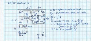
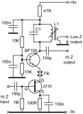
On the right are the circuit diagram of a simple cascode IF amplifier and hand drawn graph paper layout viewed from the underside (solder side) with some explanatory notes. The PC layout uses double sided fibreglass board with maximum ground plane area on each side.
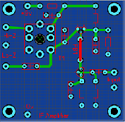

On the right are the underside view in green and top (component) side view in blue of the completed PC board. In each case the majority of the copper areas are inter-
The completed board is 2 inches by two inches (50.8 x 50.8mm) and no attempt was made to reduce the overall size in this simple example.
All holes are through plated. The corner mounting holes are connected to ground and will accept 8BA or M2 bolts. The holes for PC connecting pins will accept single or double sided Vero splined PCB pins.
The overall gain is 30-
AGC arrangements are left to the constructor and will depend on the required dynamic range. Possible options are direct control of each stage current or multiple shunt PIN diodes -
The amplifier as shown will work on a 9v supply but the dynamic range can be increased by running it on a 15v supply. However, do check the collector/drain current is not too high on that increased voltage.