ON7YD
3.5MHz ARDF
 transmitter
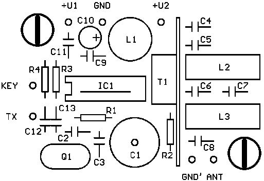
Partlist
| IC1 : CD4001 | T1 : IRF610 | Q1 : 3.5...MHz | L1 : 5µH |
| L2 : 26 wind. * | L3 : 24 wind. * | R1 : 1M8 | R2/3/4 : 15k |
| C1 : 10-60pF | C2/3 : 150pF | C4 : 100n | C5 : 330p |
| C6 : 1n5 | C7 : 120p | C8 : 1n | C9 : 10n |
| C10 : 10µ/25V | C11 : 100n | C12/13 : 10n |
* : L2 and L3 = 0.5mm CuL wire on Amidon T50-6
back to top of this page
Functional description
For ARDF competitions on 80 meter a transmitter is needed that has :
- 1 to 5 Watt HF
- high efficiency (battery operated)
- simple and relyable
- sufficient harmonic surpression
- constant power for antenna-impedances between 20 and 100 Ohm
- handle any SWR (up to 100 % reflection)
With a supply voltage of 12 to 13 Volt this transmitter has a HF power of about 3 Watt. By increasing the supply voltage of the PA to 30 Volt a HF power of 20 Watt can be produced.
Function
This transnsmitter is designed as a classic 3 stage TX :
The OSCILLATOR is build arround gate A of IC1. R1, C2 and C3 act as the feedback network and with C1 the frequency can de adjusted a few kHz. By pulling the connection 'TX' to ground the oscillator is started. By replacing the crystal Q1 by a 3.58mhz ceramic resonator the frequency can be adjusted about 50kHz with C1. With C1 the frequency can only be increased, so the frequency range is from 3.58MHz to 3.63MHz. To get the complete range below 3.6MHz a small inductor in series with C1 is needed. The disadvantage of a ceramic resonator is a reduced frequency stability. If temperature changes are avoided (mount T1 on a sufficient large heatsink) and C2 and C3 are 'NP0' condersors a good frequency stability can de acieved. Due to variations between different crystals it might be nessecary to replace C3 by a smaller avlue (10 to 100pF) if the oscillator is not running stable. Also if using a ceramic resonator adjustment of C3 can be required.
The DRIVER is very straightforward. The 3 remaining gates of IC1 are put in parallel. They act as a buffer between the oscillator and PA and also provide a sufficient drive current for the PA. By pulling the connection 'KEY' to ground the transmitter is keyed. NEVER KEY THE TRANSMITTER IF THE OSCILLATOR IS NOT RUNNING !!! In this case T1 will shortcircuit the supply voltage. The FET might survive this, but most likely the power supply and/or L1 will not.
As PA a fast switching FET in is used in classe C. the PA has an effienciency of 60 to 70% and the FET is almost indestructable. For antenna impedances between 20 and 100 Ohm the output power is almost constant. C4 seperates the DC voltage from the antenna, with the network C5, L2, C6, L3, C7 and C8 a sufficient harmonic surpression and antenna matching is achieved.
The connection '+U1' is for te supply voltage of IC1 (maximum 15 Volt) and '+U2' for the supply voltage of the PA (maximum 30 Volt).
Components
L1 must be suitable for peak currents of 1A. L2 and L3 are respectively 26 and 24 windings of 0.5mm CuL equally spread over a T50-6 toroidal core (Amidon). If you want to use other toroidal cores you will have to experiment with the number of windings. Take into account that the material of the core not only determines the inductance but also has an influence on the harmonic surpression. If you cannot measure the harmonic surpression you are advised to stick to the T50-6 cores.
C10 is a tantal, take care of polarisation and voltage !
T1 has to be mounted on a small heathsink. If the supply voltage exceeds 15V the heathsink should be larger..
Output power and harmonic surpression
The output power and efficiency in function of of '+U2', with '+U1' = 12V and a antenna impedance of 50 Ohm (measured with Rohde&Schwarz URV3) :
| '+U2' | output power | efficiency |
|---|
| 10V | 1.9W | 60% |
| 11V | 2.4W | 60% |
| 12V | 2.9W | 61% |
| 13V | 3.3W | 62% |
| 15V | 4.8W | 65% |
| 18V | 7.1W | 70% |
| 25V | 13W | 72% |
| 30V | 19W | 73% |
Output power and efficiency dependent on the antenna impedance, with '+U1' and '+U2' = 13V (measured with Rohde&Schwarz URV3) :
| ant. imp. | output power | efficiency |
|---|
| 100 Ohm | 2.7W | 60% |
| 50 Ohm | 3.3W | 62% |
| 33 Ohm | 3.4W | 59% |
| 20 Ohm | 3.5W | 57% |
Harmonic surpression, with '+U1' en '+U2' = 13V, crystal frequency 3.58MHz and antenna impedance 50 Ohm (measured with Rohde&Schwarz FSEA) :
| frequency | power level | BIPT norm * |
|---|
| 7.16MHz | -10dBm | 0dBm |
| 10.74MHz | -33dBm | 0dBm |
| 14.32MHz | -38dBm | 0dBm |
| 15MHz - 30MHz | less than -50dBm | 0dBm |
| above 30MHz | less than -50dBm | -26dBm |
* : BIPT = Belgian Institute for Post and Telecommunication
Use as ARDF transmitter
- If the transmitter is used with a 12 Volt battery '+U1' and '+U2' can be connected together.
- If the transmitter is not active the oscillator should be switched off ('TX' disconnected from ground), otherwise the oscillator can be heard upto 5 meters from the transmitter.
- If the oscillator is not running the power consuption is minimal, so the supply voltages do not have to be switched during a competition.
back to top of this page
Circuit diagram
 A high resolution TIFF file of the circuit diagram is included in the download package.
back to top of this page
A high resolution TIFF file of the circuit diagram is included in the download package.
back to top of this page
Printed Circuit Board
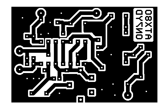
 The exact dimensions of the PCB are 1.95 x 1.30 inch (49.5 x 33.0 mm).
A high resolution TIFF file of the PCB is included in the download package.
back to top of this page
Download
Click here to download a ZIP-file that contains :
- high resolution Printed Circuit Board (TIFF file)
- PCB component layout (TIFF file)
- high resolution circuit diagram (TIFF file)
- complete functional description and manual (WORD document)
- terms of usage and disclaimer (ASCII file)
Click here to download a ZIP-file that contains the gerber files (bottom layer and drill).
back to top of this page
You are visitor number  since 21 feb. 2000