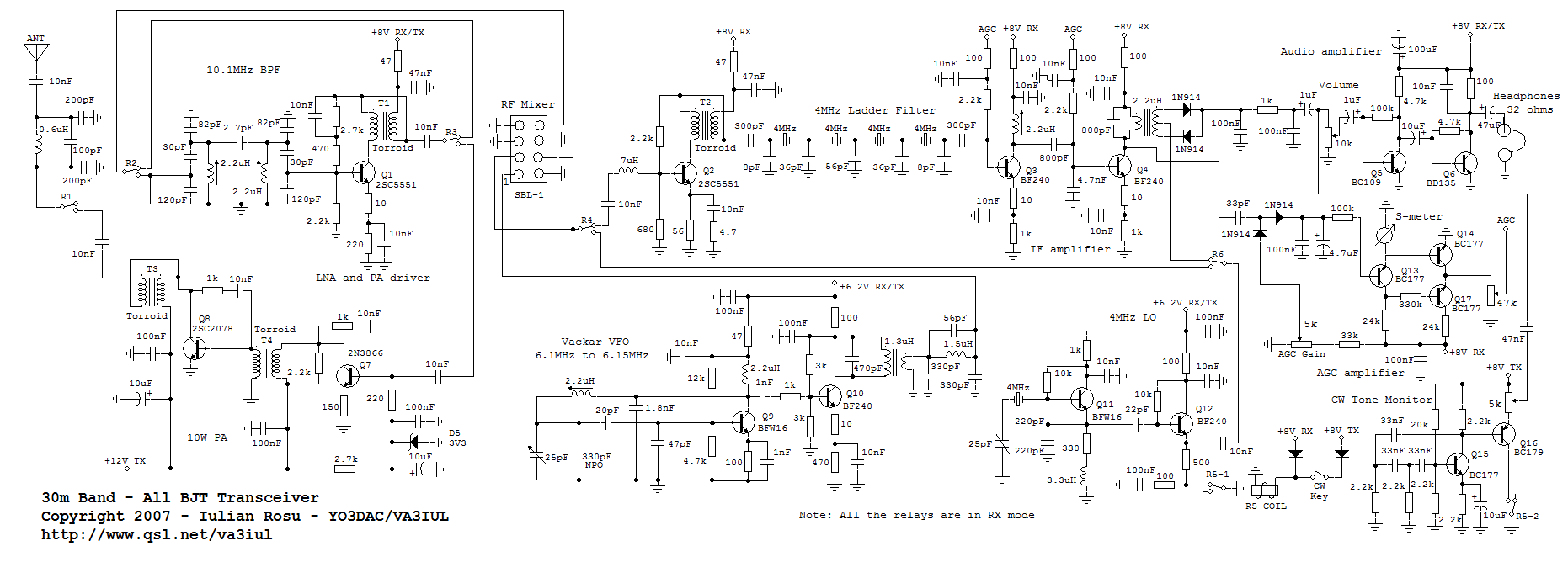
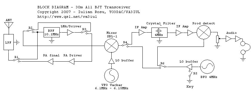
30m Band - All BJT Transceiver
Iulian Rosu - YO3DAC / VA3IUL - http://www.qsl.net/va3iul/
Reason building this radio is to get a real portable QRP transceiver with low power consumption.
On receive, the current consumption is approximately
100mA, and no more than 1.8A in TX mode, at full power.
Schematic description:
In
receive mode the signal from the antenna passes the antenna switch (R1) and goes
through the RF Band Pass Filter to the LNA input (Q1). This stage is used also
in TX mode as an RF driver. The switching between modes of the LNA is done using
two relays, R2 and R3. The gain of the stage is approximately 15dB, providing
also good IP3 performance at 20mA current consumption. The
2SC5551 could be
replaced with
BFW16 or
BFR96.
The next stage is the RF mixer (SBL-1) which translates the 10.1MHz RF frequency
to the 4MHz IF frequency.
The Variable Frequency Oscillator used for mixing is a Vackar type oscillator.
The main characteristic of this oscillator is a very good frequency stability
and good phase noise (measured phase noise was -119dBc @ 1kHz from the carrier). The
reason of this good performance is because on this type of oscillator the parametric variables of the transistor
are isolated from the LC resonator, and they do not overload it.
The output of
the VFO is low, which makes necessarily to use a buffer amplifier to boost the
generated signal. The level necessarily for mixing is approximately +7dBm.
Using very high quality components, the stability of this oscillator could be
close to a Crystal Oscillator. The oscillator transistor (Q9) is a medium power
transistor (BFW16) supplied at low Vcc to provide the best phase noise.
Q2 is the first IF stage and is using a high IP3 transistor (2SC5551 or BFW16).
The crystal ladder filter was made from 4 identical, low cost 4 MHz crystals. The
3dB band pass frequency of the filter is less than 1 kHz.
The gain of the last two IF stages (Q3, Q4) is controlled by the AGC line. The
AGC amplifiers are Q13, Q14 and Q17.
The product detector was made using two 1N914 diodes (or anything equivalent).
The headphone audio amplifier provides enough power to hear the signal into any
normal low impedance headphones.
Q15 and Q16 are the CW Tone monitor.
Q11 is the BFO on 4MHz and is followed by a buffer (Q12). Q12 is keyed in TX mode by the
CW key through the R5-1 relay. R5-1 is the only relay on this schematic that is
located in
“normal open” position in RX mode.
In TX mode the 4 MHz signal from the keyed LO, feeds the RF mixer (the same
SBL-1 used by the receiver). The relays R4 and R6 should provide both together
good isolation, better than 100 dB at 4 MHz, to don't get feedback from output
to the input of the IF amplifier.
The up converted signal at the output of the RF mixer goes through the same BPF
and RF stage (Q1) used by the receiver.
Q7 and Q8 is the driver respectively the final stage of the transceiver,
providing approximately 10W. Q8 is working in class C and should be mounted on a proper
heat sink.
Substitutions for 2SC2078 transistor are: 2SC1969,
2SC1971, 2SC1972.
For best isolation between stages and modes all the relays should be separate
one from each other. Don’t use multiple contacts relays. Cheap
signal relays SPDT
(Single Pole Double Throw) would be fine. Only R5 is a DPDT (Double Pole
Double Throw) to switch the LO buffer and the audio tone generator in the same
time.
-T1= Bifilar 2x 10 turns, tor
FT-37-43
-T2= Bifilar 2x 12 turns, tor FT-37-43
-T3=Bifilar 2x 10 turns, tor FT-50-43
-T4=Bifilar 2x 10 turns, tor FT-37-43
-Product Detector transformer: Primary=2.2uH, Secondary bifilar 2x 5turns,
IF ferrite can
-VFO transformer: Primary=1.3uH, Secondary 5 turns, IF ferrite can