High Frequency VCO Design and Schematics
Iulian Rosu, YO3DAC – VA3IUL, http://www.qsl.net/va3iul/
This note will review the process by which VCO (Voltage Controlled Oscillator) designers choose their oscillator’s topology and devices based on performance requirements, components types and DC power requirements.
Basic oscillator design specifications often require a given output power into a specified load at the design frequency. The drive level and bias current set the fundamental output current and the oscillation frequency is set by the resonator components.
Transistor selection of the transistor should consider noise, frequency, and power requirements. Based on the particular device, the design may account for parasitics of the device affecting resonator components as well as nonlinear performance specifications.
All the VCO schematics presented below were practical build using the Infineon SiGe transistor BFP420, and any of them can be re-tuned for different frequency ranges changing varicaps and LC tank values.
VCO Specifications
Phase Noise varies typically by 3dB with temperature, in the –55ºC to +85ºC range.
VCO Design Recommendations
Nonlinear Effects in VCOs
Oscillator circuit nonlinearities cause low-frequency noise components to be up-converted and to appear as noise sidebands on the VCO output. Although this statement is intuitively obvious, quantifying this mechanism is much more complex. Second-order nonlinear distortion determines the degree of noise contamination of the oscillator output for instance. Therefore, second-order distortion in the oscillator should be minimized. The degree to which any oscillator accomplishes this goal can be judged based on the second harmonic output level of the oscillator.
A good oscillator should exhibit 2nd harmonic levels on the order of -40 dBc.
Another useful indicator of good oscillator design is the change in oscillation frequency versus DC bias reduction.
A slow reduction of the supply voltage from
nominal to the point at which oscillation just ceases, should result in a very
small frequency change (for example, should be on the order of about of 20 kHz
for a well-designed 2 GHz oscillator).
The oscillator excess open-loop gain (which is
necessary for initial oscillator build-up) should be minimized in order to
prevent amplitude fluctuations from being converted into significant frequency
fluctuations.
The 2nd harmonic currents in the oscillator sustaining stage can
appear in phase quadrature with the fundamental current, thereby worsening the
conversion of AM noise to PM noise.
Ideally, the 2nd and 3rd harmonic frequencies should be placed well above the fT cut-off frequency of the oscillator sustaining stage transistor, thereby minimizing this effect.
In many VCOs, the spectral purity is dominated by AM to FM conversion mechanisms near the carrier frequency. One method to predict the AM-to-FM conversion effect in a varactor-tuned VCO is based on a simple observation of the VCO output frequency oscillator signal amplitude. A change in the RF voltage amplitude across the tuning varactor normally affects the observed tuning capacitance value in the resonator, thereby providing one substantial AM-to-FM conversion mechanism in the oscillator.
Other VCO impairments including injection locking,
load pulling, and power supply frequency pushing can cause serious oscillator
performance degradation, particularly in phase-locked systems. If the induced
impairments fall within the closed-loop bandwidth of the system, potentially
chaotic spectral behavior can result. Design margins must be identified and held
for each of these potential problem areas.
Injection Locking
Injection locking can be shown that when a signal of sufficient amplitude and sufficiently small frequency error is impressed on a free-running oscillator. Over time, the free-running oscillator changes its frequency to that of the impressed signal with a corresponding change in its signal phase and amplitude. Normally, injection locking is a very undesirable situation, but it has been used to advantage on occasion such as in narrowband bit synchronizers.
Load Pulling
VCO load pulling refers to the change in oscillator
frequency that occurs when the oscillator load impedance is changed. If this
impedance change is dynamic in nature, load pulling of the oscillator leads to
direct frequency modulation of the oscillator. Obviously, if the VCO is
contained within a phase-locked loop and the frequency of modulation lies within
the closed-loop bandwidth, unwanted interactions can result.
One of the most serious load pulling situations that can occur in practice
arises in modulators where the modulation signal causes (low-frequency) baseband
frequency modulation of the load.
In this situation the load reflection coefficient, become a function of the modulation signal.
Frequency Pushing
VCO frequency pushing is the technical term applied to the oscillator frequency perturbations that result from small changes in the oscillator's supply voltage(s). These perturbations can result from a number of factors including changes in device capacitance values caused by modified reverse biased junction capacitances, changes in the oscillator self-limiting signal mechanism, and changes in the sustaining stage gain.
Oscillator frequency pushing can lead to substantial phase noise degradation because any power supply noise directly can lead to frequency modulation of the oscillator.
Varactor Diode Nonlinear Effects
One of the main nonlinear VCO elements, particularly
in wideband VCOs, is the varactor diode. The potentially large voltage swing
across the varactor(s) leads to departures in the frequency tuning curve from
nominal and up-conversion of low-frequency noise components that contribute to
VCO phase noise sidebands.
It can be shown that minimal varactor distortion occurs when the VCO tuning
varactors are used in the back-to-back topology. Second-order distortion is
theoretically reduced to zero when matched abrupt junction varactor diodes are
used in this configuration.
Back-to-back varactor diode configuration is used to improved balance and to minimize even-order varactor nonlinearities.
Varactors should be placed at minimum voltage swing in the resonator.
Resistors should be placed about the varactors in order to maintain reverse bias and have their noise voltage short-circuited through an inductor.
In order to lower the VCO Phase Noise, a number of design rules should be respected:
There is a trade-off between the Q factor of the oscillator, its size and its price. The low Q-Factor of an LC tank and its component tolerances needs careful design for phase noise without individual readjustment of the oscillators.
Usually a larger resonator will have a higher Q (e.g. a quarter wavelength coaxial resonator).
A bipolar transistor biased at a low collector current will keep the flicker corner frequency to a minimum, typically around 6 to 15 KHz (Most semi-conductor manufacturers can provide the frequency corner (fc) of their devices as well as the 1/f characteristic.
In order to increase the power at the input of the oscillator, the current has to be increased. However, a low current consumption is critical to preserving battery life and keeping a low fc. In a practical application, the current will be set based on output power required to drive the system (typically a mixer), and then the Phase Noise will need to be achieved through other means.
- The abrupt tuning diodes will provide a very high Q and will also operate over a very wide tuning voltage range (0 to 60 V). The abrupt tuning diode provides the best phase noise performance because of its high quality factor.
- The hyperabrupt tuning diodes, because of their linear voltage vs. capacitance characteristic, will provide a much more linear tuning characteristic than the abrupt diodes. These are the best choice for wide band tuning VCO's. An octave tuning range can be covered in less than 20 V tuning range. Their disadvantage is that they have a much lower Q and therefore provide a phase noise characteristic higher than that provided by the abrupt diodes.
CAD analysis can be used to chose the varactor diode doping profiles for linear frequency tuning even in the presence of large signals.
This is the most challenging compromise because the thermal noise from the equivalent noise resistance of the varactor works together with the tuning gain of the VCO to generate phase noise. This compromise will be the limiting factor determining the phase noise performance.
Tuning line resistance should be kept very low, thereby keeping Johnson noise effects to minimal.
Any reduction in sensitivity of the tuning curve to signal amplitude is desirable because this leads to a corresponding decrease in AM to FM conversion within the oscillator.
In BJT VCOs, the amount of feedback to the emitter from the collector must not result in base-emitter junction voltage breakdown (critical point for most microwave transistors).
Oscillator self-limiting mechanism should be
implemented such that the resonator Q is not degraded. Actual limiting occurs
across the base-emitter junction rather than the base-collector junction.
The collector supply currents should be inserted with negligible resonator
loading.
Varactors should have minimum coupling to the tuned circuit, just enough to achieve an adequate frequency swing.
The tuning voltage should not be zero or the diode may be forward biased during part of the oscillator cycle and degrade performance.
The supply for the VCO should be regulated and decoupled and the oscillator should be shielded.
A suitable buffer circuit should isolate the VCO from any load.
VCO Topologies
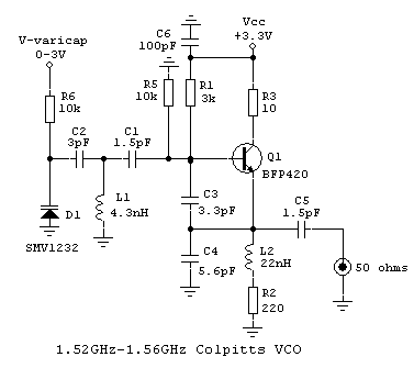
Parallel Tuned Colpitts VCO
There are 3 types of BJT Colpitts VCOs. Common-Collector, Common-Emitter and Common-Base.
The most used is Common-Collector configuration where the output is often taken from the collector terminal, simply acting as a buffer for the oscillator connection at the base-emitter terminals.
This is the only Colpitts arrangement in which the load is not part of the three-terminal model or the oscillator equation; though care must be taken to ensure that the collector output voltage does not significantly feedback through the base-collector junction capacitance.
As an alternative, the output of the common collector could also be taken across emitter resistance Re.
Series Tuned Colpitts VCO (Clapp VCO)
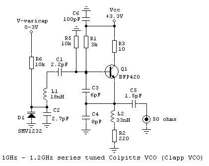
The series-tuned Colpitts circuit (or Clapp oscillator) works in much the same way as the parallel one.
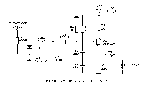
Wideband Colpitts VCO
Hartley VCO
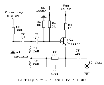
C1 is reduced to the minimum value that allows reliable starting. This is necessary because the Hartley’s lack of the Colpitts’s capacitive divider would otherwise couple the transistor capacitances to the tank more strongly than in the Colpitts, potentially affecting the circuit’s frequency stability.
Wideband Differential Push-Push VCO
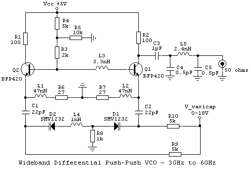
Voltage controlled push-push oscillators have
been known for some period of time, particularly because they provide a proven
design which has twice the output frequency capability of any single transistor
in a microwave VCO.
• The push-push VCO use two symmetric subcircuits to
oscillate in odd mode (180° out of phase) to the fundamental frequency fo, when
the 2nd harmonic (2fo) is coupled to the output port.
• Hence, at the output of a push-push oscillator the
fundamental signal fo and odd harmonics (3fo, 5fo,..) are canceled out, while
the even harmonics (2fo, 4fo,..) are constructively combined in-phase at the
output network, delivering the 2nd harmonic to the output load.
• Any push-push oscillator must rely on generation of signals
from each transistor that should be rich in 2nd harmonic components because the
fundamental components will cancel out. For this reason, bipolar transistors are
preferred because they have better 2nd harmonic characteristics due to inherent
non-linearities.
• As the two sub-oscillators use a common resonator and they
oscillate at halve of the output frequency, higher resonator Q-factors are
available.
• In a push-push oscillator the fundamental frequency signal
is terminated by a “virtual ground’. Thus, the loaded Q-factor is equal to the
unloaded Q-factor of the oscillator, a fact which improves the phase noise
performances of the oscillator.
• Another improvement in the phase noise is coming from the
fact that by definition, push-push oscillators provides load termination for the
2nd harmonic signal, which otherwise would be reflected back, fluctuates each
voltage of the oscillator and works as a noise power for the fundamental
oscillation, which leads to increase of the phase noise.
• Additionally, push-push oscillators are highly resistant to
load pulling effects, because the sub-oscillators are terminated by a ‘virtual
ground’ and only the 2nd harmonic frequency component is influenced by the
oscillators load impedance. This behavior will improve the frequency stability
of the oscillator.
• To obtain strong fundamental fo rejection at the push-push
output, it is very important to have a good symmetry of the circuit and of the
PCB layout.
• For temperature compensation, current mirror circuits could
be added at the emitter and the base of the transistors, but this will be done
at the expense of increasing the wideband phase noise.
Differential Cross-Coupled VCO
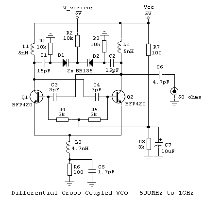
The cross-coupled differential transistor pair presents a negative resistance to the resonator due to positive feedback.
This negative resistance cancel the losses from the resonator enabling sustained oscillation.
Frequency variation is achieved with two varicap diodes BB135.
Negative Resistance VCO
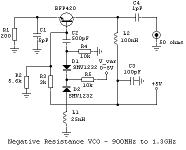
The output can be taken by capacitive coupling at the emitter (low level) or at the collector (higher level, but have more spurious).
Franklin VCO
Franklin oscillator uses two transistor stages having the same common terminal (emitter for bipolar device) when the greater power gain and better isolation from the resonant circuit is possible compared with the case of a single-stage configuration.
There are two possible configurations for the resonant circuit, parallel and series. The circuit presented below uses a parallel LC resonant circuit (L1 and the varctor diode).
In the case of a parallel resonant circuit configuration, the resonant LC circuit is isolated from the input of the first stage and the output of the second stage by means of small shunt capacitances C1 and C2 having high reactances at the resonant frequency.
In this circuit, each stage shifts phase 180° so that the total phase shift is 360° which is equivalent to zero phase shift. We may say that one stage serves as the phase inverting element in place of the RC or LC network which generally performs this function. It is, from an analytical viewpoint, immaterial which stage we choose to look upon as amplifier or phase inverter. The configuration is essentially symmetrical in this respect; both stages provide amplification and phase inversion.
The salient feature of the Franklin oscillator is that the tremendous amplification enables operation with very small coupling to the resonant circuit.
Therefore, the frequency is relatively little influenced by changes in the active device, and the Q of the resonant circuit is substantially free from degradation.
The closest approach to the high frequency stability inherent in this oscillator is attained by restriction of operation to, or near to, the Class-A region. This should not be accomplished by lowering the amplification of the two stages, but, rather by making the capacitors C1 and C2 very small.
Additionally, a voltage-follower 'buffer' stage is helpful in this regard. Extraction of energy directly from the resonant tank, would, of course, definitely negate the frequency stability otherwise attainable.
Obviously, the Franklin oscillator is intended as a low-power frequency-governing stage, not as a power oscillator.
Goral VCO
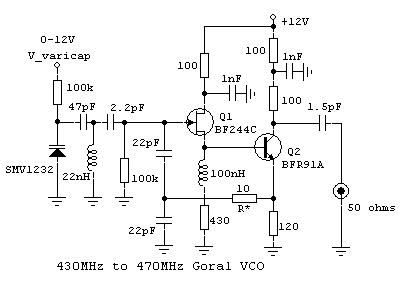
The Goral VCO has an emitter-follower stage inserted in the feedback path of an otherwise conventional Colpitts oscillator circuit.
The midpoint of the capacitive divider (which is actually part of the resonant tank) now sees a much lower impedance with respect to ground than would be the case without the emitter follower.
Because the feedback gain of a Goral VCO is greater than a standard Colpitts, placing a feedback resistor R*, helps improving the overall phase noise performance and improving also the linearity, reducing the VCO generated harmonics.
The power gain of the JFET/BJT combination is much greater than that of the JFET 'oscillator' alone. There is latitude for considerable experimentation in the ratio of the two capacitors used in the Colpitts section of the circuit. This ratio can be optimized for frequency stability without easily running out of feedback.
Note that the emitter-follower is directly coupled to the JFET. It may be necessary to experiment with bias-determining resistances to ascertain Class-A operation from the emitter-follower. Also, the output transistor is intended to operate in its Class-A region.
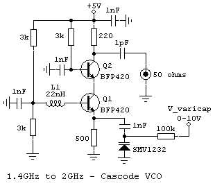
Cascode VCO
To provide higher isolation of the load from the VCO resonant circuit a cascode VCO configuration, can be used.
The negative resistance oscillation conditions for common emitter transistor Q1 are provided by using the feedback inductance L1.
Vackar VCO
And here is the winner. If you want to build a very stable, low phase noise, and low spurious VCO, definitely Vackar VCO is the choice.
This is not a common type in the RF “professional” world; one reason could be the name of its inventor.
A Vackar VCO is a variation of the split-capacitance oscillator model. It is similar to a Colpitts or Clapp VCO in this respect. It differs in that the output level is more stable over frequency, and has a wider bandwidth when compared to a Colpitts or Clapp design.
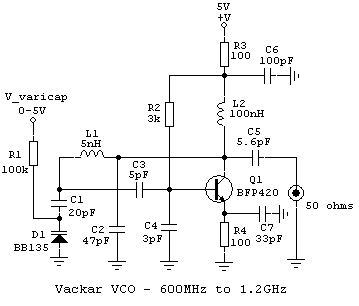
• The Vackar oscillator is a
modified Clapp oscillator with additional variable capacitor Cv (varicap
capacitance). It combines the features of the circuits with the series and
parallel arrangements and is useful for very
wideband frequency tuning.
The configuration of the Vackar oscillator shown in figure above demonstrates
the main difference compared with the Clapp schematic.
The capacitance C3 represents the phase-varying capacitance providing an
additional phase shift.
• With the circuit of the Vackar oscillator, it is
possible to utilize the maximum value of the oscillator quality factor over the
complete tuning range, and the circuit has substantially constant output
amplitude.
• The Vackar VCO circuit incorporates a π-section tank to attain the needed 180° phase-reversal in the feedback loop.
However, the inverted feedback signal is not directly fed back to the input of the active device; rather, it is loosely coupled through a small capacitor. Often, a shunt capacitor is introduced to further reduce the coupling.
The basic idea is to isolate the resonant circuit as much as possible from the input of the active device, consistent with obtaining reliable oscillation.
This circuit is particularly advantageous with solid-state devices, and especially with bipolar transistors that have inordinately-low input impedances and that present a widely-varying reactance to the tuned circuit as a consequence of temperature and voltage changes.
Once the overall circuit is operational, the values of capacitance C1 in series with Cvar and collector capacitance (C2) may be optimized for best stability. Generally, it will be found that the capacitor closest to the collector of the transistor can be several times larger than the capacitor associated with the base circuit.
The introduction of attenuation in the feedback loop (via the small capacitor in the Vackar) prevents over-excitation and effectively isolates the resonant circuit from the active device.
The frequency tuning range of Vackar VCO is above one octave, not observable to many oscillator types.
The frequency tuning is provided independently of the coupling to the LC tank circuit.
The parametric variables of the transistor (which depends by the bias current and temperature), are isolated from the resonator.
The transistor input is not overloaded as other VCO circuits and the collector output has low impedance providing low gain just to maintain the oscillation.
The feedback division ratio is fixed (typical range for coupling ratio is 1:4 up to 1:9). Even if the VCO is tuned, the impedance divider is fixed, in this way increasing the stability.
Two negative sides of Vackar VCO are the critical starting oscillation point, and the low output level, which always requires to use a buffer amplifier. When the oscillation doesn’t start means that it doesn’t have enough positive feedback, as for to begin the oscillation and maintain it in the time. In the above schematic C3 and C4 are critical values finding this point.
L2 is used as an RF choke with SRF outside of the frequency range, to don’t affect the tuning range and flatness over frequency. It is important that the RF choke in the collector circuit 'looks good' at the operating frequency (presents a high inductive reactance). Resonances from distributed capacitance in the choke windings, especially those in the series-resonant mode, can degrade stability or even inhibit oscillation. Ferrite-core chokes are generally suitable for this application. Sensitivity to RF choke characteristics is common to all oscillator circuits that use chokes for shunt-feeding the DC operating voltage to the oscillator.
References:
1. Alpha Industries - VCO Application notes
2. Minicircuits - VCO Application notes
3. Oscillator Basics and Low-Noise Techniques for Microwave Oscillators and VCOs - U.Rohde
4. Oscillator Design and Computer Simulation - R.Rhea
5. RF and Microwave Transmitter Design – A. Grebennikov
6. RF and Microwave Transistor Oscillator Design – A. Grebennikov
7. Practical Oscillator Handbook - I. Gottlieb
8. Frequency Synthesizers Design Handbook - J.A.Crawford
9. RF Design Magazine - 1997 - 2003
10. Microwave Journal - 1997 - 2008
11. Microwaves & RF - 2002 - 2006