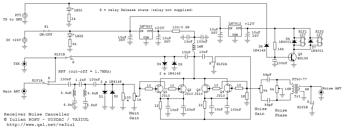
Receiver Noise Canceller
Iulian Rosu , YO3DAC / VA3IUL, http://www.qsl.net/va3iul
Receiver Noise Cancellers, using an additional receive antenna (diversity antenna) to phase out the local noise, were invented during the tube era, before WW2.
The main antenna receives both, the desired signal and the noise. The noise canceller works by combining the noise received from the Main Antenna and the noise received from the Noise Antenna (which is 180° out of phase with the desired received signal), thus canceling the noise and leaving only the desired signal.
Important to mention that the two antenna outputs (main and noise) are combined after modifying their phase AND amplitude (the relative signal levels).
The interference waveform must be continuous and reasonably stable in its shape and amplitude, as most of the noise from industrial, residential, computers, and power lines is.
Finding
the most effective Noise Antenna for a required frequency band and your specific
situation is experimental.
Several manufacturers make this kind of noise cancellers for radio amateurs
(S.E.M., MFJ, WiMo, Timewave, DX Engineering). Their block diagram is almost the
same, but the approach of the circuit implementation is different. Whatever
complexity their circuit has, the noise canceling performances are pretty
similar.
Unfortunately all of these devices suffer from dealing with high input signals.
The noise
canceller presented bellow mainly improves the IP3 linearity of the circuit.
Improved
linearity is done by using on each antenna path (main and noise) two J310 JFETs
in parallel which are supplied at relative high DC voltage (+20V).
Compared to a single J310 JFET supplied at +12V, a stage using two JFETs in
parallel supplied at +20V have more than 6dB better IP3 performance. Also this
approach has higher gain and lower noise figure, parameters which are important
for a first stage amplifier in a receiver system.
The signal from the main antenna is routed to the circuit through a steep
elliptic High Pass Filter with cut-off at 1.7 MHz, filter which rejects strong
broadcast stations and high noise levels below that frequency. Further, the
signal is amplified by the Q1, Q2 stage.
The signal from the Noise antenna it goes initially to the phase changer
circuit, and later amplified by the stage Q3, Q4 JFETs.
Drains of all JFETs Q1, Q2, Q3, and Q4 are connected together, connection where
we get the sum of the Main and Noise signals.
Tuning
the Noise Gain and Noise Phase potentiometers, attain the noise null.
Also,
adjusting the amplitude and the phase of the signals coming from the Main and
Noise antennas, you can get an enhancement of the desired received signals. This is an
advantage which otherwise you get if using two paralleled receivers connected to
different antennas. This is an option that some high-price transceivers have.
For any
noise canceling circuit to work
properly, very important is to use for the “Noise” antenna an antenna similar
with the "Main" antenna. Some manufacturers mistakenly mention that the “Noise”
antenna should be a simple wire or a simple loop antenna. Generally can be used
any “Noise” antenna type (even a simple random length wire) but I found that the best performances were obtained when
the antennas are similar in size and especially when they have the same polarization. The main
explanation of that the antennas should be similar, is because the Noise doesn’t have to be local in origin; it can also
arrive by ionospheric propagation from distant sources. This effect can allow
noise from sources very far away to accumulate at the receiving location and
"mask" the weak signals.
If both antennas (main and noise) are resonant antennas and not a simple wire, the distance between them should be λ/2 or greater. Sometime, due to limited space, this distance is hard to get in 80m and 40m, but the circuit it will work sufficient well even the antennas are closer.
The noise canceling
performance is not affected much by the distance between antennas, but the
desired signal enhancement option will be affected.
On the schematic, the two relays are shown in receive mode, which means: Switch
1 is closed, and the PTT of the transceiver is not pushed (PTT line not
connected to the ground). R state of the relays means release state (when the
circuit is not DC supplied, and Switch 1 is open).
For the
reliability of the circuit it is very important to use fast
signal relays, with switching (operate) time less than 5msec (most of the
modern signal relays does this).
Important to don’t damage the circuit with high RF power is: Never transmit with
the transceiver if the PTT line from the transceiver is not connected to the
circuit. If forget to do this connection and transmit 100W, the JFETs
Q1,Q2,Q3,Q4 and diodes D3, D4 will be most probably damaged (due to high level
of standing waves inside of the box). To prevent this situation I placed the
LED1 into the circuit, to check always if the PTT cable coming from the
transceiver is connected to the circuit. When the PTT from the transceiver is
not pushed (RX mode), most of the transceivers put +8V on the PTT line. This DC
voltage is used to light on the LED1.
For minimum loss of TX power when passing through the noise canceller circuit,
on the back panel of the device place the TRX connector near the Main antenna
connector, and place the relay RLY1 between them. Use short 50 ohms coax cables
(4mm diameter with PTFE dielectric).
Never place the Noise Canceller circuit after a high power amplifier (more than
100W).
If use an external Transmatch, I would recommend placing the Noise Canceller
circuit between the Transmatch and the Antenna, even some manufacturers
recommend to be placed between the Transceiver and the Transmatch.
Also I recommend to tune the Transmatch (internal or external) with the Noise
Canceller circuit not DC supplied (Switch 1 open), and switch ON the device after the tuning
is done.
The
phasing transformer Tr1 was made on a
FT50-77
ferrite toroid, having 16 turns on primary and 4 turns on secondary. Another
option is
BN-43-3312.
Here is a short movie which shows the performance of the Noise Canceller device. Can be seen on the waterfall the noise reduction and improved signal readability when the device is active or is not.
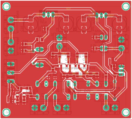
PCB Layout