Modifications for the Kenwood
TS-940

19-07-1998 TS-940S LCD Clock Display Erratic
Operation
We have received a few reports concerning erratic
operation of teh LCD clock display when the Main dial is rotated, or the VBT or
SLOPE TUNE controls are operated. This appears as if you had pressed the SET,
SCROLL, or GRAPH switches.
This erratic operation may be caused by
improper timing of the input pulses applied to the auxiliary display
microprocessor, IC1.
- This symptom is easily corrected by replacing IC2 MBM2764-30T1 with
MBM2764-30T2, on Digital Unit A. Early models of the improved IC will carry
the old nomenclature but will be distinguished by a white dot on the top of
the chip.
- After the IC has been changed reset the main microprocessor by pressing
and holding the A=B key, and then turning the power switch OFF and then back
ON. Then release the A=B key.
- After this change is made the sub-display will not immediately track the
main display. A slight delay has been introduced int he new IC to prevent any
timing errors. It may take approximately 0.5 seconds for the LCD to track the
main display.
- Please return the old IC2 to the Service Department along with the WSR for
Credit.
Perform this modification only if the symptom occurs, as a
repair. This change is not required otherwise.
Time required for this
modification is 1 hour or less.
19-07-1998 TS-940S SSB Talk Power
Improvement
Author: Trio-Kenwood
Communication, inc.
Service Bulletin no. 921 (22-7-1987)
TS-940S's in the serial number range of 601XXXX through 708XXXX may be
limited n SSB peak power as compared to full CW output. The level may be
increased by changing the value of capacitors C182 and C183 in the ALC circuit
on the Control board. The recommended replacement value for each capacitor is
0.0022 uF, 50v (CK45B1H222K).
Procedure:
- Disconnect the power cord and antenna from the transceiver.
- Remove the top and bottom covers (16 screws).
- Locate the Control board on the bottom of the transceiver.
- Locate transistor Q37 on the board (toward the back right hand side.) The
two capacitors are mounted on the foil side of the board underneath
Q37.
- To access the bottom of the board remove the 8 screws that mount the board
and heat sink to the chassis (See figure 1.)
- Carefully lift the board/heat sink fomr the right hand side and pivot it
toward the front of the transceiver.
- Replace C182 and C183 with 0.0022 uf, 50v capacitors.
- Lower the board back into its original position (don't pinch any wires!)
and re-install the 8 mounting screws.
- Put the covers back on the TS-940S and secure them with the 16 case
screws.
- Connect the antenna and power cord then test the transceiver for normal
operation.
 This is an optional change and may not be performed under
warranty.
This is an optional change and may not be performed under
warranty.
Time required for this change is 1 hour or less.
19-07-1998 TS-940S Erratic
display
Author: Trio-Kenwood
Communication, inc.
Service Bulletin no. 951 (20-1-1989)
Intermittent control or display problems that are difficult to correct with
the reset procedure may be caused by a faulty ROM socket. The socket should be
checked to insure that it makes good electrical contact with each pin of the
ROM. If it is found to be intermittent, remove the socket and solder the ROM
directly to the board. It should be noted that units between serial numbers
701XXXX to 811XXXX and from 903XXXX to 909XXXX are not likely to have this
failure. In addition, units with a serial number of 909XXXX and above do not
incorporate a socket.
CAUTION
Removing the socket requires good soldering skills. The ROM is mounted on the
Digital A unit and is designated as IC2. The board, being double sided, has
solder connections on both component and foil sides. When the socket is removed,
it is very important to insure that each pin is completely solder free. Having
to pry up on the socket means that it is not completely desoldered and will
cause the circuit foils to tear.
When performing any work on the Digital A board, CMOS handling techniques
must be observed. Such techniques include using a grounded or isolated soldering
tip, avoid touching the pins of IC chips with your fingers, and ground yourself
with a wrist ground strap.
To remove the socket:
- Disconnect the power cord and antenna coax.
- Remove the top and bottom covers from the transceiver.
- Remove the 2 flat head screws from each side of the front panel
chassis.
- Loosen the round head screw on each side of the front panel
chassis.
- Carefully rotate the front panel forward. It will be necessary to unplug
the VS-1 cable from the transceiver.
- Remove the 4 screws from the speaker mount.
- Carefully pull up on the mount and rotate it toward the front panel. Swing
the mount toward the right side of the transceiver and allow it to rest on the
Digital B unit shield.
- Remove the 8 screws from the Digital A unit shield plate.
- Lift the plate and rotate it to the left side of the transceiver.
- While avoiding contact with the pins, remove the ROM (IC2) and set it
aside on anti-static foam.
- Remove the 6 screws that mount the Digital A board. Rotate the board
toward the front panel to expose the bottom side of the board.
- Carefully desolder the socket and remove it from the board. Do not pry up
on the socket. If it does not easily pull off the board, the top foils are
still soldered to the socket.
- Install the ROM in the board and solder it in place.
- Assemble the transceiver by reversing steps 1 - 11. Do not pinch the power
switch cables between the front panel and the body of the
transceiver.
Time required for this modification is 1.5 hrs or less.
19-07-1998 RX AUDIO
- On Kenwood TS-904's that do not have the optional Voice Synthesizer module
VS-1 installed, you may notice a hum in the RX audio. The already present
molex connectored cable for this module should be dressed to the top of the
shield case where the voice synthesizer mounts. However, on some units they
have been left hanging free in the vicinity of the PLL and digital A units and
are quite good at picking up noise from these circuits.
- The Fix, is simply to secure this cable to the top of the shield case
where the VS-1 would mount. Plastic tie straps, or even simple electrical tape
works very nicely.
19-07-1998 Amtor switching
time
- Most stock TS-940S' require 30 to 50 mS to switch back from TX to RX. This
can be reduced to less than 20 mS by cutting the center lead of Transistor Q68
on the Control Unit PCB.
- After the modification, a slight "click" will be heard in the speaker
during switching. However, this is no big deal to the AMTOR nut because of the
improved switching time.
19-07-1998 ALC time constant
- This Mod will change the TS-940 time constant from approximately 1 second
to .022 second. This means that the ALC will no longer impose its own
characteristics on your audio response; the ALC will now follow your own
sylabbic rate and emphasis. Usually the average output will increase, which
will drive a linear amplifier harder (or at least those meters will swing
higher!!). Use caution in this mod and have another Ham-friend check around
your TX frequency for splattering while you are QRV.
- The TS-940 has a 10uF cap (C31) and 100K resistor (R104) which make up the
time constant for the ALC. This tends to reduce the output power for the
duration of the ALC time constant (or till the circuit charges up again). Then
it starts all over again on the next word.
- This procedure allows modification to the control PCB (X53-1420-11) in the
TS-940 WITHOUT having to remove the board. Remove the bottom cover and locate
the control PCB. Locate R137 and R104. These are located in the upper right
hand corner as the rig faces you upside down (near VR-3). A service manual is
helpfull for locating parts!!!
Using an Exacto knife, VERY CARFULLY scrape
off some insulation from the top of these two resistors. Now tack-solder a 1/8
watt 2.2k ohm resistor from the top of one of these resistors to the top of
the other. The time constant is now changed. Reassemble and enjoy a superb
rig.
19-07-1998 TS-940 Mod for MARS and all band
operations
Locate IC number 109.
Now find diode 130 and cut it
for all-band transmit.
If you want just MARS coverage, locate IC 111 and
112, and snip diode 135 beside it.
15-04-2000 TS-940S PLL
unlock
Author: Trio-Kenwood
Communication, inc.
Service Bulletin no. 900 (18-10-1985)
Some users of the TS-940S have reported a blanking of the display accompanied
by a loss of transmit and receive. Readjustment of the PLL unit will correct
this tendency.
Procedure:
- Set the Dial frequency for approximately 1.8 MHz (inside the
band).
- Using an RF probe at TP5 adjust L22, L23, and L24 for a maximum reading on
the meter. You should see approximately 250 mV.
- Adjustment of L24 will produce the greatest change, which may be up to a
90° adjustment from its present position.
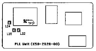
Time required for the procedure is .5 hour or less.
15-04-2000 TS-940S Antenna Tuner
Relays
Author: Trio-Kenwood
Communication, inc.
Service Bulletin no. 907 (4-4-1986)
Occasionally during operation of the AT-940 a VSWR greater than 1.5 to 1
might cause overloading of the relay contacts in the antenna tuner. This may be
especially noticeable when switching BANDS, or if TUNINS is performed too
frequently. The following procedure should reduce or eliminate the tendency.
Parts Required
Q69: Digital transistor, (DTC124ES)
R304: 5,6 Kohm 1/6 Watt Resistor,
(RD14BB2C562J)
Procedure:
- Add the circuit as shown below.
- After the circuit has been installed adjust VR4 for a 10-15 watt output
when the antenna tuner operates.
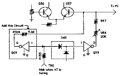
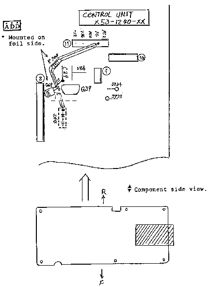
Time required for the modification is 1 hour or less.
15-04-2000 TS-940S PLL
unlock
Author: Trio-Kenwood
Communication, inc.
Service Bulletin no. 908 (8-4-1986)
Reports of a PLL unlock on the lower frequencies may be due to low VCO
levels. The following change will increase the VCO level and should prevent
reoccurrence of this symptom.
Parts required
C168, change to 15 pF 50V (CC45SLIH150J)
Procedure:
- On the RF unit (X44-1660-00) change C168 from a 33 pF capacitor to a 15 pF
50V capacitor.
- Readjust the VCO BPF (RF unit L74-76) according to the instructions
contained in the TS-940 Service manual.
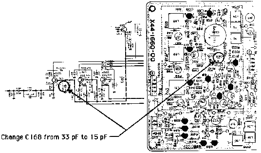
This change is applicable to units prior to serial number 606xxxx.
Time
required for this modification is 1 hour or less.
15-04-2000 TS-940S AVR unit capacitor
change
Author: Trio-Kenwood
Communication, inc.
Service Bulletin no. 909 (8-4-1986)
In those areas of the country that are subject to large power line voltage
fluctuations, excessive voltage may be applied to capacitor C12 on the AVR unit
(X43-1500-00). These voltage fluctuations might exceed the capacitor breakdown
voltage. Replacing capacitor C12 with a capacitor having a higher breakdown
voltage will help prevent this potential problem.
Procedure:
On the AVR unit (X43-1500-00) change C12 from a 6800 µF capacitor to a 5600
µF 25 V capacitor (C90-2037-05)
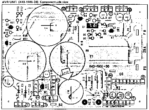
This change is applicable to serial numbers prior to 701xxxx.
Time
required for this modification is 1 hour or less.
15-04-2000 TS-940S AGC circuit
improvements
Author:
Trio-Kenwood Communication, inc.
Service Bulletin no. 910 (3-6-1986)
The following changes will improve the adjacent rejection of the TS-940S when
a relatively strong nearby signal is present (s-4 or above).
The AGC switch should remain in the SLOW position for all but high speed data
communications. Most CW operations will also benefit from operation in the SLOW
position.
Parts required:
15 Kohm ¼ watt resistor, (RD14CB2E153J)
1 µF 16V Electrolytic,
(CE04W1C010M)
1S1555 diode, (V1S1555)
.047 µF capacitor, (C91-0119-05)
Procedure:
RF unit
- Remove jumper wire JP7 and replace it with the parallel combination of the
15 Kohm resistor and the 1S1555 diode. Pay close attention to polarity.
- Add the 1 µF capacitor as shown in the diagram.
IF unit
Change capacitor C75 from a 1 µF 50V capacitor to a .047 µF 50V capacitor.
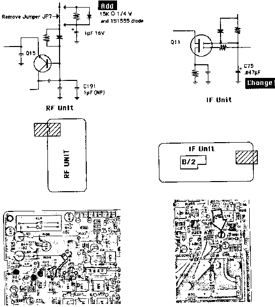
Time required for this modification is 1 hour or less.
15-04-2000 TS-940S Signal to noise ratio
improvement
Author: Trio-Kenwood
Communication, inc.
Service Bulletin no. 913 (28-6-1986)
The following change will reduce the tendency of the Zener diode in the Noise
Blanker circuit to cause an increase in the ambient noise level. This change
measures that no current flows thru this diode in the normal receive position.
Parts required:
560 ohm 1/½ watt resistor, (RD14CB2E561J)
Procedure:
On the IF unit (X48-1430-00) change R23 from 330 ohms to 560 ohms.
This change will be incorporated in all models beginning with serial number
603xxxx.
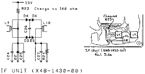
Time required for this modification is 1 hour or less.
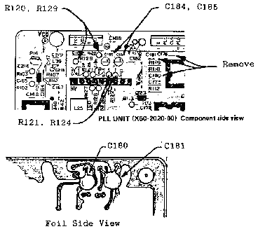
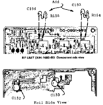
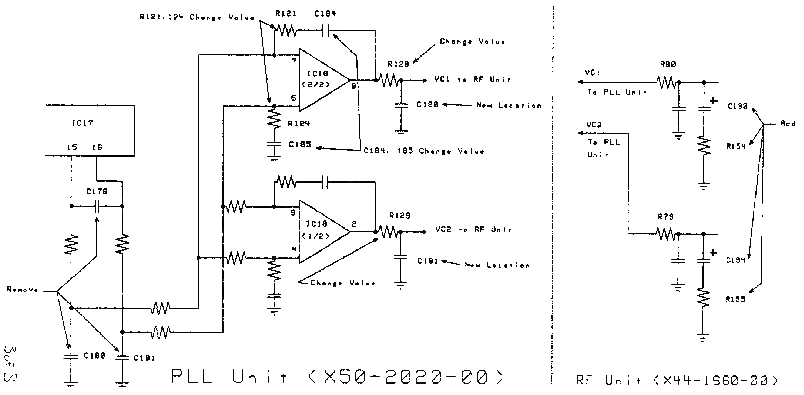
15-04-2000 TS-940S VCO carrier to noise
ratio improvement
Author:
Trio-Kenwood Communication, inc.
Service Bulletin no. 917 (2-3-1987)
The Carrier to Noise ratio of the TS-940S may be improved by the following
changes. This bulletin supersedes bulletin number 911 dated September 15, 1986.
Parts required:
PLL UNIT (X50-2020-00)
R120, 129     3.3 Kohm 1/6 watt carbon resistor     RD14CB2C332J
R121, 124     680 ohm 1/6 watt carbon resistor      RD14CB2C681J
C180, 181     .01 µF disc ceramic capacitor         C91-0117-05
C184, 185     .33 µF 35V Tantalum capacitor         CS15E1VR33M
RF UNIT (X44-1660-00)
R154, 155     3.9 Kohm 1/6 watt carbon resistor     RD14CB2C392J
C193, 194     1 µF 25V Tantalum capacitor           CS15E1E010M
Procedure:
On the PLL unit (X50-2020-00) remove capacitor C176, C180, and C181. Change
resistor R120 and R129 from 470 ohms to 3.3 Kohm. Change resistor R121 and R124
from 1 Kohm to 680 ohms. Change capacitors C184 and C185 from .22 µF to .33 µF
35V tantalum capacitors. Install C180 and C181 in the positions shown in the
accompanying diagrams. The use of new capacitors is recommended to improve
reliability, don't try to reuse the old capacitors! Capacitors C181 and C180
should be attached to the foil side of the PLL unit.
On the RF unit (X44-1660-00) install the series RC circuit composed of R154
and C193, and R155 and C194, as shown in the accompanying diagrams. As the
diagrams illustrate it is easiest to move C132 and C193 to the foil side of the
board and install the series RC circuit on the component side.
This is an optional change and may not be performed under warranty. Time
required for this modification is 1.5 hour or less.
PLL UNIT
RF UNIT
15-04-2000 TS-940S Squelch switching
noise
Author: Trio-Kenwood
Communication, inc.
Service Bulletin no. 918 (21-7-1987)
In some TS-940S below S/N 711xxxx, a "popping" or "clicking" noise may be
heard when the squelch circuit is opened or closed. This may be more noticeable
when an optional CW filter is installed. The following procedure will minimize
the noise.
Parts required:
R194        560 Kohm 1/6 watt             RD14CB2C564J
R197        220 ohm 1/6 watt              RD14CB2C221J
R355, 356   220 Kohm 1/6 watt             RD14CB2C224J
C284        0.47 µF, 50V electrolytic      C90-0484-05
Procedure:
- Disconnect the power cord and antenna from the transceiver.
- Remove the top and bottom covers (16 screws).
- Locate the I.F. board on the bottom of the transceiver.
- Remove the 7 screws from the I.F. board.
- Carefully unplug connector # 17 (right side of optional CW filter) by
prying up on the plug. Do not pull on the wires.
- Move the 4 wires (yel, org, brn, red) that run across the far side of the
I.F. unit out of the way so the board may be removed.
- Carefully lift and rotate the board toward the left side of the
transceiver to expose the foil side of the board.
- Using a small craft knife, cut the foil at the 3 points shown in figure 1.
(top right corner of the board).
- Unsolder and discard resistors R194 and R197. They are mounted on the
component side of the board and soldered on the foil side.
- Install a 560 Kohm resistor on the component side of the board as shown in
figure 2. This resistor is now designated as R194.
- On the foil side of the board, add the 3 resistors (R197, 355, 368) as
shown in figure 3.
- Add a small jumper wire as shown in figure 3.
- Add capacitor C282 as shown in figure 3. Observe polarity and insulate the
positive (+) lead with shrink tubing.
- Carefully place the board in its original position (do not pinch wires)
and secure it with the 7 screws.
- Plug in connector # 17. Move the 4 wires on the far side of the board back
to their original position.
- Put the covers back on the TS-940S and secure them with the 16 case
screws.
- Connect the antenna and power cord then test the transceiver for normal
operation.

This is an optional change that may not be performed under warranty. Time
required for this modification is 1 hour or less.
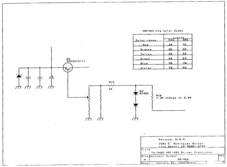
21-04-2000 TS-940S MRF-485 Driver Transistor
Notes
Author: Kenwood
Communication, inc.
Service Bulletin no. 988 (16-1-1992)
Some MRF-485 transistors are being supplied by Motorola with a Green or Blue
color ranking. If these transistors are installed without modifying the driver
bias circuit there is a strong possibility that they will fail within a very
short time frame.
These high gain transistors cause the circuit to become unstable which can
cause the circuit to break into self oscillation, and therefore self-destruct.
Recommendations:
Use of Red, Orange, or Yellow hfe color rankings is recommend. These lower
gain transistors work just fine and do not suffer from the circuit instability
problem. If you are only able to obtain the high gain transistors you will need
to modify the varistor/temperature compensation circuit on the final unit
(X45-1400-00) by changing R16 from 1.2 Kohm to 2.2 Kohm.
During its production the TS-940S used two different varistor values. The
original part was an STV3H(O). It was changed in mid-production to an SV-03YS.
R15 was changed from an 820 ohm resistor to a 1 Kohm resistor at the same time.
Therefore the countermeasure differs depending upon the serial number of the
radio.
| Serial number lot
| Varistor
| R15
| R16
| MRF485 Green or Higher rank |
| 106xxxx or earlier |
STV3H(O) |
820 |
1.2 K |
See "Caution below" |
| 107xxxx or later |
SV03YS |
1 K |
2.2 K |
Change R16 from 1.2 to 2.2 K |
Caution: If using a Green or higher hfe rank one of the above
countermeasure must be taken depending upon the serial number of the set. After
replacing the drivers check the bias current. We recommend transmitting for 1
hour in SBB mode with no modulation into a dummy load. After this time frame
check the bias current. It must not exceed 300 mA on the original radio. If the
current changes you must change R16 from 1.2 Kohm to 2.2 Kohm.