|

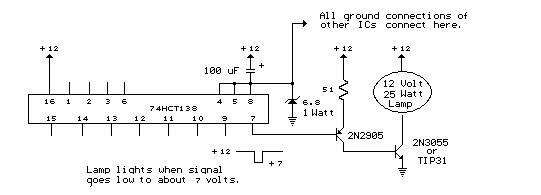
Interfacing 5 volt CMOS
to 12 volt/ 25 Watt Loads

The circuit below is
designed to be used with the bi-directional lamp sequencer shown above on
this same page. Two additional transistors are used to increase the
current from the 74HCT138 decoder to control 12 volt 25 watt lamps. A 6.8
volt/1 watt zener diode is used in series with the ground connection of
all the CMOS ICs (74HC14, CD4516 and 74HC138s) so that the total voltage
across the CMOS devices will be about 5.2 volts and the outputs will move
from +12 to about +7 when selected. The 2N2905/PNP transistor stage is
connected as an emitter follower which provides a high impedance to the
decoder output and supplies about 80 mA of current to the base of the
2N3055 NPN power transistor which then supplies 2 or more amps to the 12
volt lamp. The voltage across the PNP transistor will be about 7 volts
when it is turned on and the heat dissapation will be about 0.6 watts.
That should't require a heat sink if several lamps are sequencing but it
may get quite warm if the circuit is idle on a single output. The 2N3055
power transistor operates as a switch and drops very little voltage (less
than 0.5) when conducting, and will not require a heat sink. Other
transistors may be substituted such as the TIP29 or TIP31 for the 2N3055
and most any medium power (500mA) PNP for the 2N2905.
Original scheme edited by Bill
Bowden, http://www.bowdenshobbycircuits.info
Variable 3 - 24 Volt / 3
Amp Power Supply
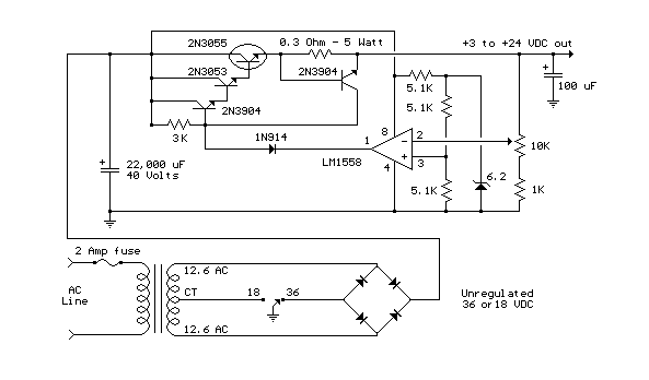
This regulated power
supply can be adjusted from 3 to 25 volts and is current limited to 2 amps
as shown, but may be increased to 3 amps or more by selecting a smaller
current sense resistor (0.3 ohm). The 2N3055 and 2N3053 transistors should
be mounted on suitable heat sinks and the current sense resistor should be
rated at 3 watts or more. Voltage regulation is controlled by 1/2 of a
1558 or 1458 op-amp. The 1458 may be substituted in the circuit below, but
it is recommended the supply voltage to pin 8 be limited to 30 VDC, which
can be accomplished by adding a 6.2 volt zener or 5.1 K resistor in series
with pin 8. The maximum DC supply voltage for the 1458 and 1558 is 36 and
44 respectively. The power transformer should be capable of the desired
current while maintaining an input voltage at least 4 volts higher than
the desired output, but not exceeding the maximum supply voltage of the
op-amp under minimal load conditions. The power transformer shown is a
center tapped 25.2 volt AC / 2 amp unit that will provide regulated
outputs of 24 volts at 0.7 amps, 15 volts at 2 amps, or 6 volts at 3 amps.
The 3 amp output is obtained using the center tap of the transformer with
the switch in the 18 volt position. All components should be available at
Radio Shack with the exception of the 1558 op-amp.
Original scheme edited by Bill
Bowden, http://www.bowdenshobbycircuits.info
Variable Voltage and
Current Power Supply
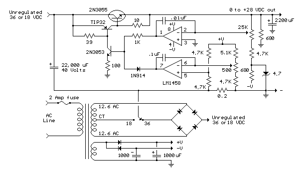
Another method of using
opamps to regulate a power supply is shown below. The power transformer
requires an additional winding to supply the op-amps with a bipolar
voltage (+/- 8 volts), and the negative voltage is also used to generate a
reference voltage below ground so that the output voltage can be adjusted
all the way down to 0. Current limiting is accomplished by sensing the
voltage drop across a small resistor placed in series with the negative
supply line. As the current increases, the voltage at the wiper of the 500
ohm pot rises until it becomes equal or slightly more positive than the
voltage at the (+) input of the opamp. The opamp output then moves
negative and reduces the voltage at the base of the 2N3053 transistor
which in turn reduces the current to the 2N3055 pass transistor so that
the current stays at a constant level even if the supply is shorted.
Current limiting range is about 0 - 3 amps with components shown. The
TIP32 and 2N3055 pass transistors should be mounted on suitable heat sinks
and the 0.2 ohm current sensing resistor should be rated at 2 watts or
more. The heat produced by the pass transistor will be the product of the
difference in voltage between the input and output, and the load current.
So, for example if the input voltage (at the collector of the pass
transistor) is 25 and the output is adjusted for 6 volts and the load is
drawing 1 amp, the heat dissipated by the pass transistor would be (25-6)
* 1 = 19 watts. In the circuit below, the switch could be set to the 18
volt position to reduce the heat generated to about 12 watts.
Original scheme edited by Bill
Bowden, http://www.bowdenshobbycircuits.info
2 Watt Switching Power
Supply
In this small switching
power supply, a Schmitt trigger oscillator is used to drive a switching
transistor that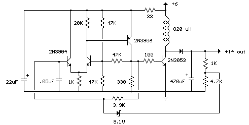 supplies current to a small inductor. Energy is stored in the inductor
while the transistor is on, and released into the load circuit when the
transistor switches off. The output voltage is dependent on the load
resistance and is limited by a zener diode that stops the oscillator when
the voltage reaches about 14 volts. Higher or lower voltages can be
obtained by adjusting the voltage divider that feeds the zener diode. The
efficiency is about 80% using a high Q inductor.
supplies current to a small inductor. Energy is stored in the inductor
while the transistor is on, and released into the load circuit when the
transistor switches off. The output voltage is dependent on the load
resistance and is limited by a zener diode that stops the oscillator when
the voltage reaches about 14 volts. Higher or lower voltages can be
obtained by adjusting the voltage divider that feeds the zener diode. The
efficiency is about 80% using a high Q inductor.
Original scheme edited by Bill
Bowden, http://www.bowdenshobbycircuits.info
DC to DC Converter
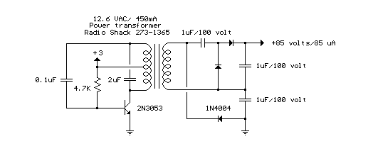 Here
is a DC to DC converter using a standard 12 VAC center tapped power
transformer and a single bi-polar NPN transistor. The circuit is not very
efficient but will produce a high voltage usable for low power
applications. The input battery voltage is raised by a factor of 10 across
the transformer and further raised by a voltage tripler consisting of
three capacitors and diodes connected to the high voltage side of the
transformer. The circuit draws about 40 milliamps and should operate for
about 200 hours on a couple of 'D' alkaline batteries. Higher voltages can
be obtained by reducing the 4.7K bias resistor. Here
is a DC to DC converter using a standard 12 VAC center tapped power
transformer and a single bi-polar NPN transistor. The circuit is not very
efficient but will produce a high voltage usable for low power
applications. The input battery voltage is raised by a factor of 10 across
the transformer and further raised by a voltage tripler consisting of
three capacitors and diodes connected to the high voltage side of the
transformer. The circuit draws about 40 milliamps and should operate for
about 200 hours on a couple of 'D' alkaline batteries. Higher voltages can
be obtained by reducing the 4.7K bias resistor.
Original scheme edited by Bill
Bowden, http://www.bowdenshobbycircuits.info
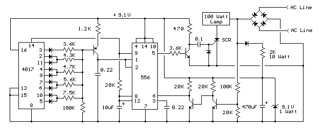
Varying brightness AC
lamp
In this circuit, an SCR
is used to slowly vary the intensity of a 120 volt light bulb by
controlling the time that the AC line voltage is applied to the lamp
during each half cycle.
Caution:
The circuit is directly connected to the AC power line and should be
placed inside an enclosure that will prevent direct contact with any of
the components. To avoid electrical shock, do not touch any part of the
circuit while it is connected to the AC power line. A 2K, 10 watt power
resistor is used to drop the line voltage down to 9 volts DC. This
resistor will dissipate about 7 watts and needs some ventilation.
Operation:
A couple NPN transistors are used to detect the beginning of each half
cycle and trigger a delay timer which in turn triggers the SCR at the end
of the delay time. The delay time is established by a current source which
is controlled by a 4017 decade counter. The first count (pin 3) sets the
current to a minimum which corresponds to about 7 milliseconds of delay,
or most of the half cycle time so that the lamp is almost off. Full
brightness is obtained on the sixth count (pin 1) which is not connected
so that the current will be maximum and provide a minimum delay and
trigger the SCR near the beginning of the cycle. The remaining 8 counts
increment the brightness 4 steps up and 4 steps down between maximum and
minimum. Each step up or down provides about twice or half the power, so
that the intensity appears to change linearly. The brightness of each step
can be adjusted with the 4 resistors (4.3K, 4.7K, 5.6K, 7.5K) connected to
the counter outputs.
The circuit has been
built by Don Warkentien (WODEW) who suggsted adding a small 47uF capacitor
from ground to the junction of the current source transistor (PNP) to
reduce the digital stepping effect so the lamp will brighten and fade in a
smoother fashion. The value of this capacitor will depend on the 4017
counting rate, a faster rate would require a smaller capacitor.
Original scheme edited by Bill
Bowden, http://www.bowdenshobbycircuits.info
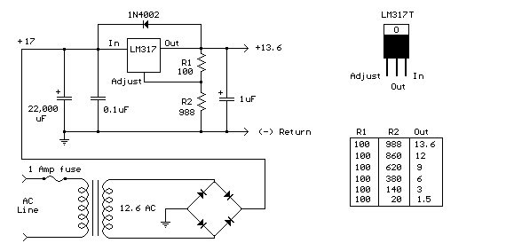
LM317T Variable Voltage
Regulator
The LM317T is a
adjustable 3 terminal positive voltage regulator capable of supplying in
excess of 1.5 amps over an output range of 1.25 to 37 volts. The device
also has built in current limiting and thermal shutdown which makes it
essentially blow-out proof.
Output voltage is set by
two resistors R1 and R2 connected as shown below. The voltage across R1 is
a constant 1.25 volts and the adjustment terminal current is less than
100uA. The output voltage can be closely approximated from Vout=1.25 *
(1+(R2/R1)) which ignores the adjustment terminal current but will be
close if the current through R1 and R2 is many times greater. A minimum
load of about 10mA is required, so the value for R1 can be selected to
drop 1.25 volts at 10mA or 120 ohms. Something less than 120 ohms can be
used to insure the minimum current is greater than 10mA. The example below
shows a LM317 used as 13.6 volt regulator. The 988 ohm resistor for R2 can
be obtained with a standard 910 and 75 ohm in series.
When power is shut off to
the regulator the output voltage should fall faster than the input. In
case it doesn't, a diode can be connected across the input/output
terminals to protect the regulator from possible reverse voltages. A 1uF
tantalum or 25uF electrolytic capacitor across the output improves
transient response and a small 0.1uF tantalum capacitor is recommended
across the input if the regulator is located an appreciable distance from
the power supply filter. The power transformer should be large enough so
that the regulator input voltage remains 3 volts above the output at full
load, or 16.6 volts for a 13.6 volt output.
Original scheme edited by Bill
Bowden, http://www.bowdenshobbycircuits.info
LM317T Voltage Regulator
with Pass Transistor
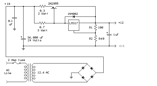 The
LM317T output current can be increased by using an additional power
transistor to share a portion of the total current. The amount of current
sharing is established with a resistor placed in series with the 317 input
and a resistor placed in series with the emitter of the pass transistor.
In the figure below, the pass transistor will start conducting when the
LM317 current reaches about 1 amp, due to the voltage drop across the 0.7
ohm resistor. Current limiting occurs at about 2 amps for the LM317 which
will drop about 1.4 volts across the 0.7 ohm resistor and produce a 700
millivolt drop across the 0.3 ohm emitter resistor. Thus the total current
is limited to about 2+ (.7/.3) = 4.3 amps. The input voltage will need to
be about 5.5 volts greater than the output at full load and heat
dissipation at full load would be about 23 watts, so a fairly large heat
sink may be needed for both the regulator and pass transistor. The filter
capacitor size can be approximated from C=IT/E where I is the current, T
is the half cycle time (8.33 mS at 60 Hertz), and E is the fall in voltage
that will occur during one half cycle. To keep the ripple voltage below 1
volt at 4.3 amps, a 36,000 uF or greater filter capacitor is needed. The
power transformer should be large enough so that the peak input voltage to
the regulator remains 5.5 volts above the output at full load, or 17.5
volts for a 12 volt output. This allows for a 3 volt drop across the
regulator, plus a 1.5 volt drop across the series resistor (0.7 ohm), and
1 volt of ripple produced by the filter capacitor. A larger filter
capacitor will reduce the input requirements, but not much. The
LM317T output current can be increased by using an additional power
transistor to share a portion of the total current. The amount of current
sharing is established with a resistor placed in series with the 317 input
and a resistor placed in series with the emitter of the pass transistor.
In the figure below, the pass transistor will start conducting when the
LM317 current reaches about 1 amp, due to the voltage drop across the 0.7
ohm resistor. Current limiting occurs at about 2 amps for the LM317 which
will drop about 1.4 volts across the 0.7 ohm resistor and produce a 700
millivolt drop across the 0.3 ohm emitter resistor. Thus the total current
is limited to about 2+ (.7/.3) = 4.3 amps. The input voltage will need to
be about 5.5 volts greater than the output at full load and heat
dissipation at full load would be about 23 watts, so a fairly large heat
sink may be needed for both the regulator and pass transistor. The filter
capacitor size can be approximated from C=IT/E where I is the current, T
is the half cycle time (8.33 mS at 60 Hertz), and E is the fall in voltage
that will occur during one half cycle. To keep the ripple voltage below 1
volt at 4.3 amps, a 36,000 uF or greater filter capacitor is needed. The
power transformer should be large enough so that the peak input voltage to
the regulator remains 5.5 volts above the output at full load, or 17.5
volts for a 12 volt output. This allows for a 3 volt drop across the
regulator, plus a 1.5 volt drop across the series resistor (0.7 ohm), and
1 volt of ripple produced by the filter capacitor. A larger filter
capacitor will reduce the input requirements, but not much.
Original scheme edited by Bill
Bowden, http://www.bowdenshobbycircuits.info
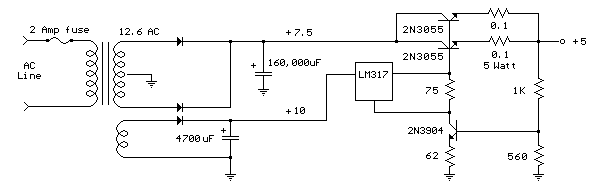
High Current Regulated Supply
Original scheme edited by Bill
Bowden, http://www.bowdenshobbycircuits.info
The high current
regulator below uses an additional winding or a separate transformer to
supply power for the LM317 regulator so that the pass transistors can
operate closer to saturation and improve efficiency. For good efficiency
the voltage at the collectors of the two parallel 2N3055 pass transistors
should close to the output voltage. The LM317 requires a couple extra
volts on the input side, plus the emitter/base drop of the 3055s, plus
whatever is lost across the (0.1 ohm) equalizing resistors (1volt at 10
amps), so a separate transformer and rectifier/filter circuit is used that
is a few volts higher than the output voltage. The LM317 will provide over
1 amp of current to drive the bases of the pass transistors and assumming
a gain of 10 the combination should deliver 15 amps or more. The LM317
always operates with a voltage difference of 1.2 between the output
terminal and adjustment terminal and requires a minimum load of 10mA, so a
75 ohm resistor was chosen which will draw (1.2/75 = 16mA). This same
current flows through the emitter resistor of the 2N3904 which produces
about a 1 volt drop across the 62 ohm resistor and 1.7 volts at the base.
The output voltage is set with the voltage divider (1K/560) so that 1.7
volts is applied to the 3904 base when the output is 5 volts. For 13 volt
operation, the 1K resistor could be adjusted to around 3.6K. The regulator
has no output short circuit protection so the output probably should be
fused.
Simple Adjustable
Voltage Source
A simple but less
efficient methode of controlling a DC voltage is to use a voltage divider
and transistor emitter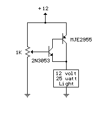 follower configuration. The figure below illustrates using a 1K pot to set
the base voltage of a medium power NPN transistor. The collector of the
NPN feeds the base of a larger PNP power transistor which supplies most of
the current to the load. The output voltage will be about 0.7 volts below
the voltage of the wiper of the 1K pot so the output can be adjusted from
0 to the full supply voltage minus 0.7 volts. Using two transistors
provides a current gain of around 1000 or more so that only a couple
milliamps of current is drawn from the voltage divider to supply a couple
amps of current at the output. Note that this circuit is much less
efficient than the 555 timer dimmer circuit using a variabe duty cycle
switching approach. In the figure below, the 25 watt/ 12 volt lamp draws
about 2 amps at 12 volts and 1 amp at 3 volts so that the power lost when
the lamp is dim is around (12-3 volts * 1 amp) = 9 watts. A fairly large
heat sink is required to prevent the PNP power transistor from
overheating. The power consumed by the lamp will be only (3 volts * 1 amp)
= 3 watts which gives us an efficiency factor of only 25% when the lamp is
dimmed. The advantage of the circuit is simplicity, and also that it
doesn't generate any RF interference as a switching regulator does. The
circuit can be used as a voltage regulator if the input voltage remains
constant, but it will not compensate for changes at the input as the LM317
does.
follower configuration. The figure below illustrates using a 1K pot to set
the base voltage of a medium power NPN transistor. The collector of the
NPN feeds the base of a larger PNP power transistor which supplies most of
the current to the load. The output voltage will be about 0.7 volts below
the voltage of the wiper of the 1K pot so the output can be adjusted from
0 to the full supply voltage minus 0.7 volts. Using two transistors
provides a current gain of around 1000 or more so that only a couple
milliamps of current is drawn from the voltage divider to supply a couple
amps of current at the output. Note that this circuit is much less
efficient than the 555 timer dimmer circuit using a variabe duty cycle
switching approach. In the figure below, the 25 watt/ 12 volt lamp draws
about 2 amps at 12 volts and 1 amp at 3 volts so that the power lost when
the lamp is dim is around (12-3 volts * 1 amp) = 9 watts. A fairly large
heat sink is required to prevent the PNP power transistor from
overheating. The power consumed by the lamp will be only (3 volts * 1 amp)
= 3 watts which gives us an efficiency factor of only 25% when the lamp is
dimmed. The advantage of the circuit is simplicity, and also that it
doesn't generate any RF interference as a switching regulator does. The
circuit can be used as a voltage regulator if the input voltage remains
constant, but it will not compensate for changes at the input as the LM317
does.
Original scheme edited by Bill
Bowden, http://www.bowdenshobbycircuits.info
Voltage Regulators
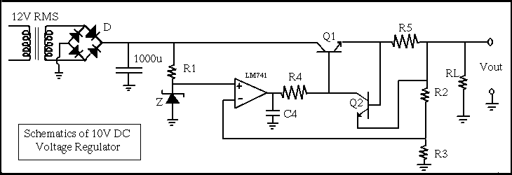
Voltage Regulators are used to change a sinusoidal AC
signal into a DC smooth signal which remains constant independent of
changes in load current.
The series-pass transistor (Q1) is used for circuits which operate at
higher current levels (typically currents higher than 100mA). The series
pass transistor acts as a common-collector amplifier, also known as an
emitter follower. The Series Pass transistor looks like it is part of the
output stage of the op-amp. The effect of adding this transistor is that
the current rating of the circuit now becomes dependent on the ratings of
the transistor, not the ratings of the op-amp as before.
The Zener diode is added to the circuit to provide a reference voltage.
The Zener diode is usually chosen so that the "Zener Voltage" is
about half of the output voltage.
| Element |
Model, value |
| D (diodes) |
1N4007 |
| Z (Zener diode) |
D1N4734 |
| R1 |
1 Kohm |
| R2 |
16 Kohm |
| R3 |
20 Kohm |
| R4 |
500 ohm |
| R5 |
3.7 ohm |
| RL |
100 ohm - open |
| Q1 |
2N3904 |
| Q2 |
2N3904 |
Ham radio Data Center - free schematics | 73s.eu - Free Ham Radio Social Network | Free HAM Directory | About me | Acronyms | CW | Data Sheets | Docs | Download | E-mail | HOME | Ham projects | Hobby circuits | Photo galery | PIC | QTH photos |
Sign in my guestbook | View my guestbook ]
© 2001 - YO5OFH, Csaba Gajdos
|