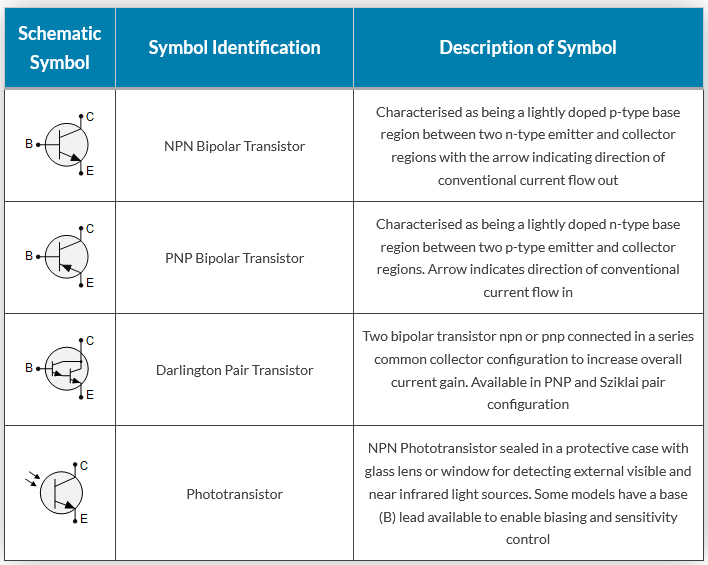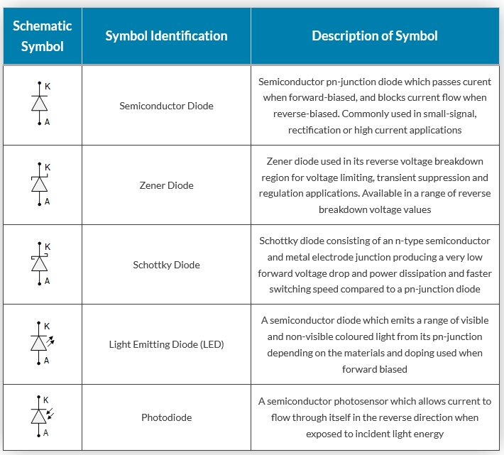
Schematic Symbols for Semiconductor Diodes
There are many different types of semiconductor devices which can be classed as a diode, and for most of these types they have a distinct circuit symbol. Some of the major diode types include here are the pn-junction, Schottky, photo diode, and light emitting diode. The schematic symbols for each of these diode types uses the same basic diode format, but is modified to indicate their different functions.
Diodes are two-terminal devices which consist of two semiconductor materials fused together to produce a pn-junction where the “n”-type material is the cathode and the “p”-type material is the anode. Generally a diodes cathode lead is identified by a coloured band.
The basic schematic symbol for a diode looks like an arrow head that points in the direction of conventional current flow from its Anode (A) terminal to its Cathode (K) terminal. The schematic symbol of a diode also shows that if forward-biased, current will flow through the direction of the arrow. However, if the polarity of the voltage is reversed, no current flows.
The schematic symbol for a zener diode and a Schottky diode are similar to that of the basic pn-junction diode except that the line representing the Cathode (K) terminal of the symbol is bent at both ends. The schematic symbol for a light emitting diode (LED) shows light energy dipicted by smaller arrows radiating from it when forward-biased.