
| ADVANCED LESSON 27 | |
| LEARNING OBJECTIVES and NOTES | |
| Solid state devices 1 | |
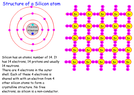
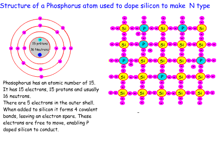
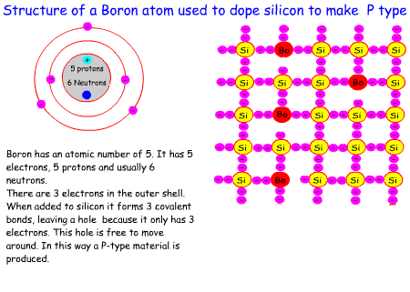
| 3n.1 Understand that doping of semiconductor material (silicon and germanium) produces p-typ (electron deficient) and n-type (electron rich) semiconductors. Our world is dominated by electronic devices. The majority of these depend on semiconductors. As the word suggests a semiconductor is somewhere between an insulator and a conductor. The two main semiconductor materials are based on silicon and germanium. In their pure state these form crystals with just enough electrons (4) in the outer layer of the atoms to form the crystal, not too many, not too few. As electronic circuits depend on the movement of electrons these are not very useful as the crystals hang on to their electrons and are almost pure insulators. The situation changes when we add small amounts of impurities. The process is called DOPING. These impurities used to dope silicon and germanium come in two forms - N-type impurities such as arsenic and phosphorus. These have 5 electrons in their outer shell. When mixed with silicon which has 4 electrons in its outer shell they result in free electrons which are negatively charged (Hence the term N-type). These turn the silicon into a good conductor. P-type impurities such as boron and gallium have 3 electrons in their outer shell. When mixed with silicon they form 3 bonds leaving one unbonded. This results in holes where an electron is missing. This is effectively makes them positively charged (Hence the term P-type) The holes can accept electrons and so electrons move from hole to hole again making P-type a conductor. The movement of electrons from hole to hole also looks like hole movement in the opposite direction. |
|
| Understand current flow in terms of electron and hole movement. So, in n-type silicon electrons move making the silicon a conductor and in P-type silicon the apparent movement of holes makes the p-type a conductor. This flow of electrons or holes is called current. On its own with no power applied there will be random movement of holes and electrons, but as holes and electrons can move in any direction there is no current flow. This is the basis on which diodes and transistors work. The next stage looks at the simplest combination i.e. p- silicon and n-silicon |
|
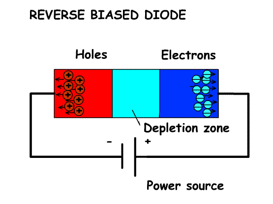
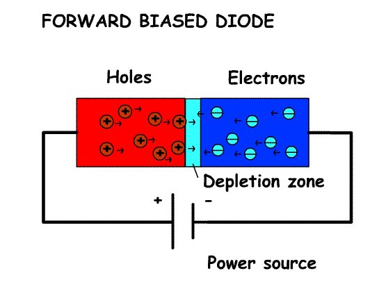
| Understand how the p-n junction forms a semiconductor diode. Understand the formation and effect of the depletion layer. Understand that an applied potential difference can cause electrons to flow across the p-n junction (forward bias) or prevent electron flow (reverse bias) depending on polarity. A diode allows current to flow in one direction only and consists of p-type silicon fused to n-type silicon. If the diode is reversed biased i.e. the n-type is connected to the positive side of a battery and the p-type to the negative side of the battery. The electrons in the n-type are attracted to the positive of the battery, the holes in the p-type are attracted to the negative side of the battery. The region between p and n silicon is called the depletion zone. It has no holes or free electrons and so forms an insulator which prevents current flowing through the diode. It should be noted that if the reverse voltage continues to be increased the depletion zone will break down and a reverse current will flow. If we now change the battery round so that the n-type silicon is connected to the negative of the battery and the p-type silicon to the positive side of the battery the electrons in the n-type are repelled by the negative of the battery and move to fill the holes in the p-type. The p-type holes are repelled by the positive of the battery and move towards the n-type silicon. The electrons fill the holes and the depletion zone becomes very narrow and fully conducting allowing the diode to conduct. In a forward biased silicon diode it takes a voltage across the diode of 0.65V before it starts to conduct. |
  |