
| ADVANCED LESSON 28 | |
| LEARNING OBJECTIVES and NOTES | |
| Solid state devices 2 | |
| 3n.2
Recall that a Zener diode will conduct when the reverse bias potential
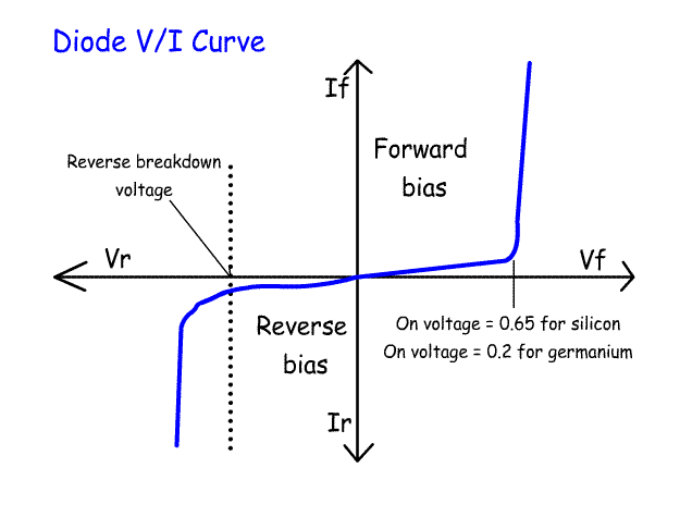
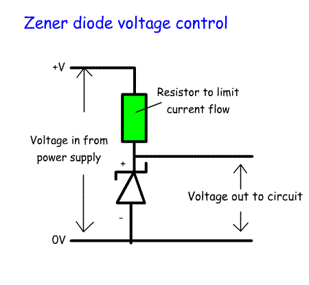
is above its designed value and identify its V/I characteristic curve. From the last lesson we understand that if the reverse bias on a diode continues to be increased the depletion zone will break down and reverse current will start to flow. The graph opposite shows the V/I curve for a normal diode. Depending on whether the diode is made of silicon or germanium as the forward bias is increased there will be a voltage where current starts to flow. For a silicon diode it is about 0.65Volts. If the diode is reverse biased, there will be a voltage where the depletion zone breaks down releasing electrons. These knock other electrons out of place causing an avalanche and current starts to flow in the opposite direction. In a normal diode this will destroy the diode. On the graph opposite the blue line shows the flow of current. If you imagine that this is someone sitting down, the knee is the point where the Reverse Voltage starts to take place. In a zener diode this reverse breakdown or avalanche voltage is controlled so that the reverse breakdown voltage can be adjusted to between 4 volts and several hundred volts. This is called the zener voltage. The zener diode is not destroyed by this process. Zener diodes are used as voltage regulators as shown in the circuit opposite. The zener is reverse biased. The supply voltage has to be greater than the output from the zener diode. If the voltage at the output rises above the zener output voltage, avalanche current will flow reducing the voltage to its set value. |
  |
| 3n.3
Understand that the depletion layer in a reverse biased diode forms the
dielectric of a capacitor and that the magnitude of the reverse bias
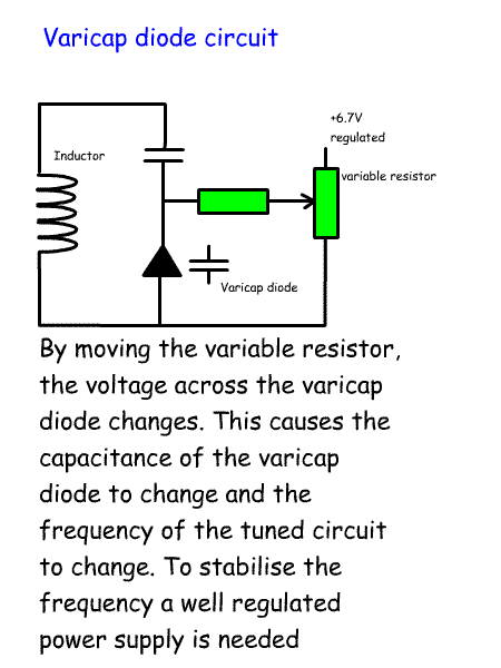
affects the width of the layer and the capacitance. If we compare a reverse biased diode to a capacitor we can think of the depletion layer as being like the dialectric and the p-type and n-type silicon as being like the metal plates. As the reverse bias is increased the depletion zone increases in size and the capacitance decreases. If the reverse bias is reduced the depletion zone becomes thinner and the capacitance increases. So, a diode can act like a variable capacitor controlled by the reverse voltage across it. This is called a variable capacitance diode. Any diode will act like a variable capacitance diode, but usually diodes are specially made to make the most of the variable capacitance effect. These diodes are used across tuned circuits to change the frequency using a potentiometer. One example is in an RIT circuits where the variable capacitance diode is switched in on receive to tune the circuit to a different frequency to the transmitter frequency. |
|