
| ADVANCED LESSON 29 | |
| LEARNING OBJECTIVES and NOTES | ||
| Solid state devices 3 | ||
|
3n.4 Understand the 3 layer model of the transistor (npn and pnp) and the channel model of the FET. The two basic types of transistor are the NPN which is made up of a piece of p-type silicon sandwiched between two pieces of N-type silicon, and the PNP which has a piece of n-type silicon sandwiched between two pieces of p-type silicon If you think about it they are like two back to back diodes. If you test a junction transistor with an ohm-meter it will appear like two back to back diodes. The symbol for a junction transistor has an arrow showing conventional current flow. So in the NPN transistor current flows from collector to the emitter. The arrow in the emitter shows this current flow. In the PNP transistor the current flows from the emitter to the collector. One down side with junction transistors is that they have a relatively low base impedance.
|
  |
|
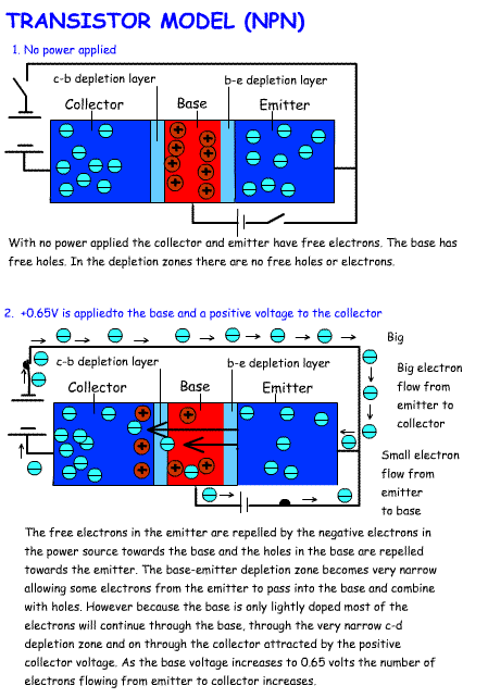
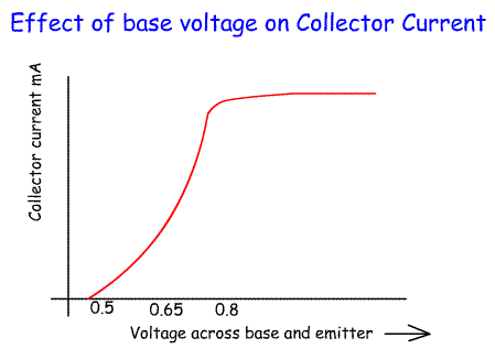
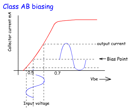
| How transistors work as switches and amplifiers A junction transistor works as shown in the diagram opposite. In a diode we looked at how the electrons move between p and n doped silicon when reverse biased and when forward biased. A transistor is formed as we outlined above from a sandwich of either PNP or NPN doped silicon. The transistor shown opposite is an NPN transistor. If you follow the notes you will see that by applying a small positive voltageto the base a small flow of electrons will take place between the emitter and base. This causes a much bigger flow of electrons to pass between the emitter and collector. Remember that when we talk about current flow we mean the opposite to electron flow. Remember Farady didn't know about electrons and decided that current flowed from positive to negative. When looking at how diodes and transistors work it is better to think in terms of electron flow. So if electrons flow from emitter to base then current is flowing from base to emitter!! If electrons flow from emitter to collector inside a transistor then current is flowing from collector to emitter!! In conclusion a small change in base voltage causes a large flow of electrons between emitter and collector. If the base voltage is DC then we can use the transistor as a switch. If the base voltage is AC then we can use the transistor as an amplifier. There are several graphs that can be plotted for transistors. The one opposite shows the effect of changing the voltage between the base and the emitter on the current flowing through the collector. At 0.5 volts the transistor is just starting to turn on. There will be a few electrons passing through to the collector causing a small collector current to flow. At 0.65 volts the collector current has increased substantially At 0.7 volts the flow of electrons has reached a maximum value and increasing the volts on the base has little effect on collector current. Another factor that will affect the collector current is the voltage applied across the collector and emitter. To investigate this a circuit is set up which will enable the base current, collector curent and emitter-collector voltage to be measured. The steps would be:
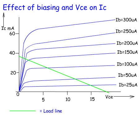
To find the saturation point connect the voltage to the collector and measure the current. To find the cut off point Saturation point: Tells you the maximum possible collector current for the circuit. Cutoff point : Tells you the maximum possible collector emitter voltage for the circuit. The graph opposite shows some typical results for a common emitter amplifier. You should be able to see that collector current depends more on the bias current than the voltage across the collector-emitter. The load line can be used to determine at what voltage to set the bias. For example if the bias is set to 100uA the collector current will be about 25mA. If an input sine wave signal swings the bias up to 150uA then the collector current will go to about 35 mA and if the bias current swings down to 50uA then collector current will go down toabout 12mA . |
   |
|
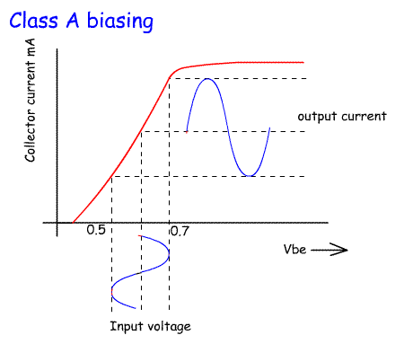
| 3n.5 Understand the basics of biasing bipolar and FET transistors (including dual gate devices). When a transistor is used as an amplifier the designers design a circuit so that there is a certain voltage on the base. This is called the bias. The bias has to be set somewhere between 0.5 and 0,7 Volts when no input is applied to the circuit. When an AC signal is applied to the base via a capcitor then the AC signal will be added to or taken away from the bias voltage. So, for example, if the AC input has a voltage that swings between + 0.1 and -0.1 volts this will cause a 0.6 voltage on the base to swing between 0.5 V and 0.7 V. As the graph opposite shows this voltage swing will cause a similar change in the collector current. |
  |
|
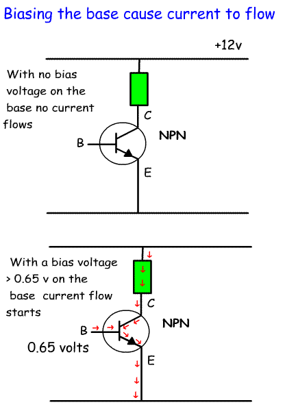
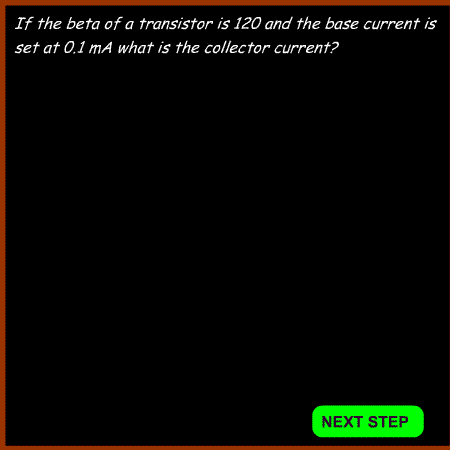
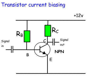
In an NPN transistor, if the collector is connected to the positive supply and the emitter to the negative supply and the base is left unconnected then no current will flow. If a small bias voltage is connected to the base (above 0.65 volts for a silicon transistor) then a small amount of current will flow from the base to the emitter. This will cause a larger current to flow from the collector to the emitter. So a small base current causes a larger collector current in other words we have a potential for amplification. For small signal transistors the beta of a transistors is the collector current divided by the base current. Beta values can range from 70 to 450. The formula showing the relationship between the current in the transistor base, the current in the collector and the beta of a transistor is: 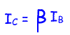 Example 2 If the base current of a transistor is set at 0.4mA and the collector current is 25mA what is the beta of the transistor? 25 = beta x 0.4mA beta = 25/0.4 beta = 63 The bias voltage on the base is very important in determining the type (or class) of amplifier. There are several different methods used to bias the base of a transistor. The 3 common systems used are: Current biasing This uses two resistors. The resistor RB is selected to provide a voltage on the base sufficient to cause base emitter current to flow. The voltage of the signal in will either add to the voltage increasing base emitter current and hence collector emitter current or reduce the base emitter current and hence collector emitter current. If too negative the signal could turn off the transistor. The disadvantage of current biasing is that the biasing voltage and current can vary during operation. Resistor values are calculated from the beta value given for the transistor. If the beta value is different, and this can happen, then the bias produced may not allow the transistor to operate in the active region. This could result in no bias current and effectively the transistor is turned off.
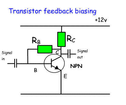
Here RB is connected between the base and the collector. If the collector current increases the collector voltage drops. This reduces the base voltage and therefore the base and collector current. This arrangement is more stable than current biasing.
It ensures that the transistor always operates in the active region,
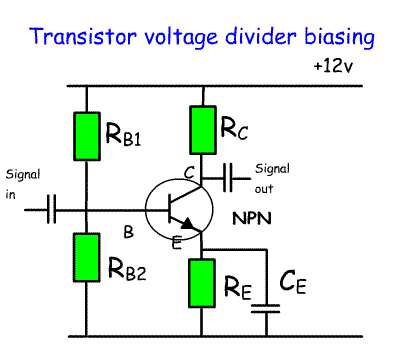
even if the beta of the transistor is different to that expected. This is one of the most common forms of biasing found in well designed transistor circuits. Resistors are chosen for the voltage divider network RB1 and RB2 so that RB2 has a current flowing through it of 10 times the base current. This arrangement is very stable and does not result in changes in base voltage. The Capacitor CE allows ac signals to pass through. So, at ac the emitter is effectively at ground potential, but at DC it stops the passage of signals, forcing dc current to flow through the resistor.
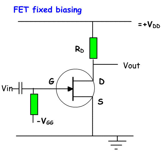
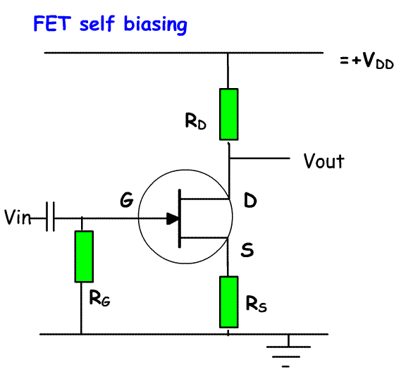
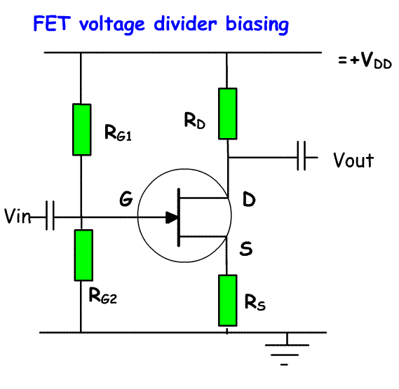
3 types of bias used: Fixed bias The negative potential required, -VGG, by the gate is provided by a battery. This ensures that the gate is always negative with respect to the source. The resistor allows an input signal to develop an input voltage on the gate. No current is drawn from the battery as no current flows from gate to source. When the FET is turned on, current flows from +VDD through RD through the drain to source and then to earth. The voltage developed across RD is used as the output. One downside of this form of biasing is the need to provide two DC supplies or a battery. Self biasing This is the most common form of JFET biasing. A voltage drop across RS means that the Source is positive with respect to earth. RG is selected provide a gate voltage which is negative with respect to the Source. When the FET is turned on, current flows from +VDD through RD through the drain to source, through RS and then to earth. The voltage developed across RD is used as the output. Voltage divider biasing Instead of a single gate resistor, a potential divider is set up using an additional resistor RG1. Resisters are selected for the divider so that the gate is negative with respect to the source |
 Example 1
       |