IN3OTD's web site
...under perpetual construction.

Wideband bias-tee
I was looking for a bias-tee to do some measurements on active devices and came across the nice design from Gary Johnson. Its performances seemed quite respectable for a relatively simple circuit, only I was looking for something that could handle some more current.
So, as a starting point for my own design I decided to analyze a bit more in detail his design to better understand how the components values influence the bias-tee performances.
Original design
In his writeup he goes into the details of the design and the effect of the components parasitics, so I won't repeat that here.
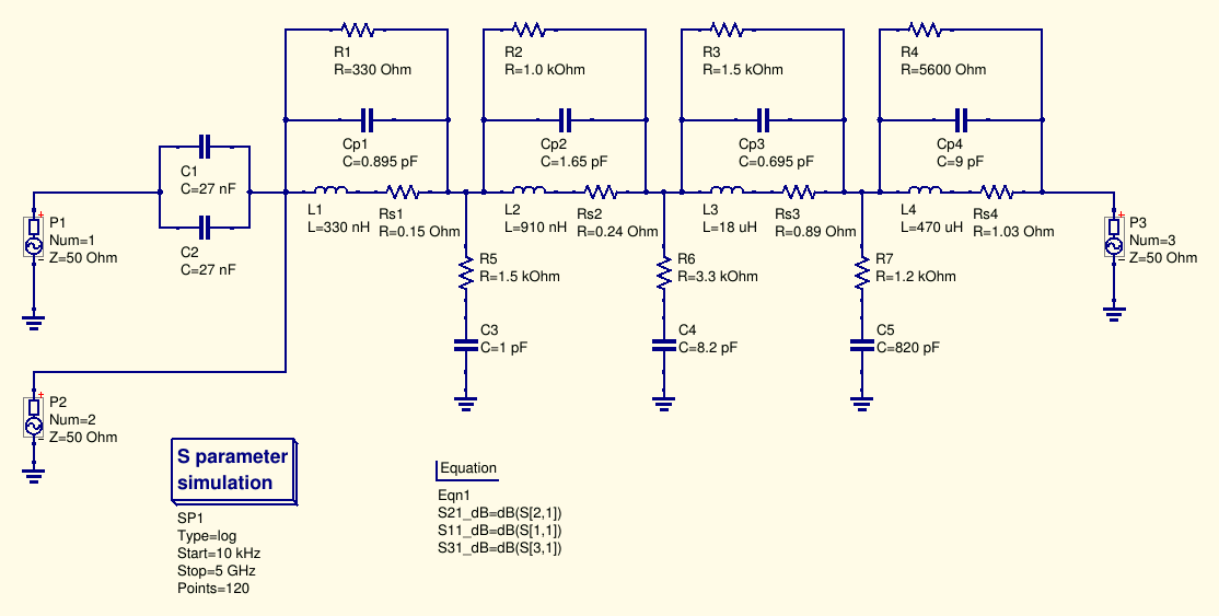
As I usually I use Qucs for simulating my amateur radio RF circuits, I copied the LTspice schematic shown at the beginning of his design report to check if the simulation results were the same also in my environment (otherwise that would very likely mean I made an error while copying the component values and computing their parasitic).
Here is the schematic entered into Qucs:
 and the following picture shows the simulation results, compared with the data show in the graphs of Gary's original writeup.
To extract the data from his graphs, I used the nice Engauge Digitizer tool, which allows to quickly obtain a file with all the data in tabular for from an imported graph picture. Qucs then has also the ability to read text data from a file and convert them into his own dataset format, to be used for further processing.
In the graphs below the curves in green were obtained from Gary's graphs while the red ones are the actual simulation results with Qucs.
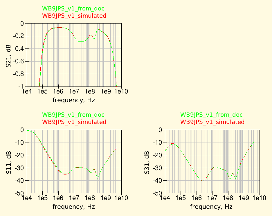 Note the very good agreement between the Qucs simulation and the original curves; that means the Qucs schematic agrees with the original LTspice schematic.
Optimized design
At this point I was curious to understand if the design could be improved; its performances are already quite good, but there is still some ripple in its attenuation/return loss/isolation curves. Gary points out in his report that he already spent a fair amount of time optimizing the component values and when I tried to further improve the design by trial and error I quickly realized how time consuming the process is and how difficult is to simultaneously improve all the three main parameters (attenuation, input return loss and isolation), since the effect of one component change affects differently all the parameters.
Of course optimization, especially by trial and error, is better left to computers, so I started thinking about writing a little script that could automatically write a Qucs netlist, run the Qucs circuit simulator to obtain the circuit performances and then decide on how to update the schematic values to attain the desired goal.
I already had an idea of what tools to use; the Qucs simulation engine (qucsator) is a standalone program that reads a text netlist and outputs a text file, so manipulating the input netlist is easy (another advantage of using text format as input format), the outputs can also be easily parsed and moreover the Qucs distribution already includes a qucsconv utility to convert the qucsator simulator results to a variety of formats. One of these supported formats is a Matlab matrix file, which can also be read by GNU Octave. I already knew a nice free nonlinear optimization library that can work with GNU Octave, NLopt so the choice was easy: a little Perl one-liner to update the input netlist and a short GNU Octave script to manage the actual optimization.
As is often the case, one of the main difficulties in setting up the optimization was to precisely define the optimization goal; the easily described wanted performances, "low losses", "good return loss" and "high isolation" have to be translated into actual performance numbers and maximum deviations from the desired values and, since not all the desired characteristics can be maximized at the same time, a weight between them has to be defined to tell the optimizer which one we would like to favor or, for example, how much return loss we are willing to trade to improve a little the isolation.
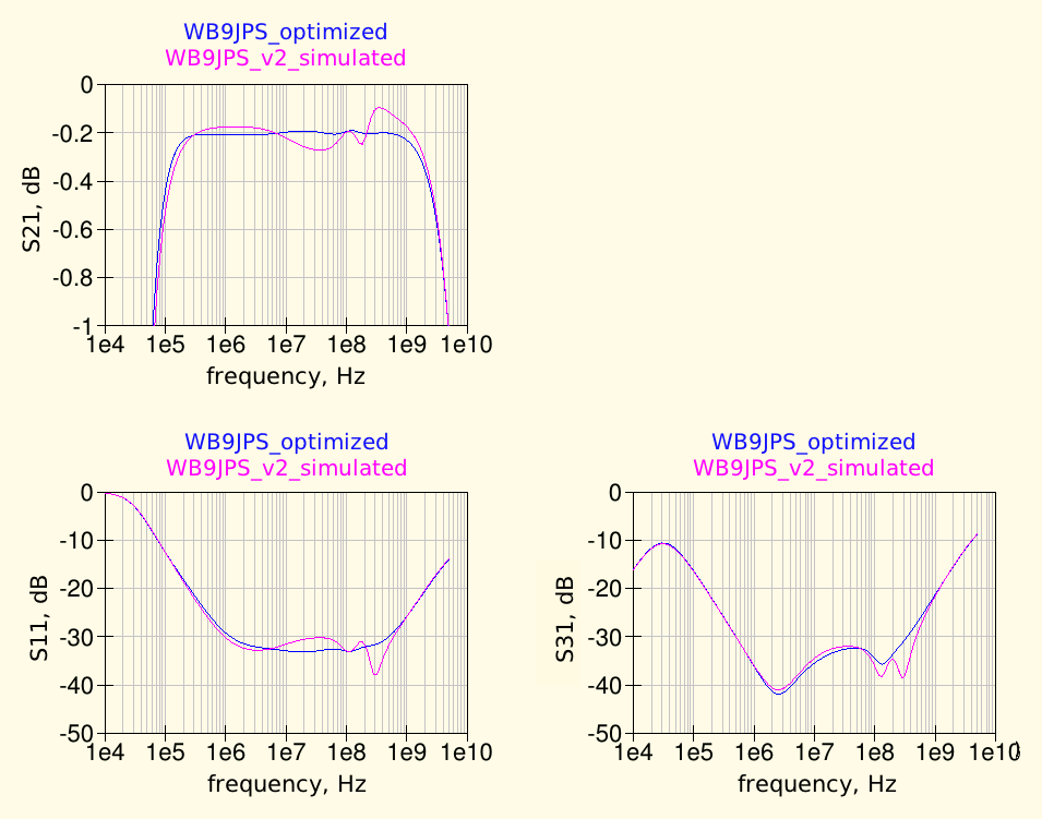
The following pictures show the bias-tee schematic with the component values optimized with the goal of having 0.2 dB of transmission losses with minimum ripple, between 300 kHz and 600 MHz. The resulting response is quite smooth across the band and has also a nice isolation.
As previously said, many other responses are possible, depending on the desired goals; in general the transmissions losses and the return loss are directly related (not so surprising...) while some more freedom seems possible in the isolation response.
 As expected, the optimized schematic performances are slightly better than the WB9JPS original design, the transmission losses are flatter, the RF return loss is also smooth and generally lower, except around 300 MHz and the isolation is still good.
Measurements
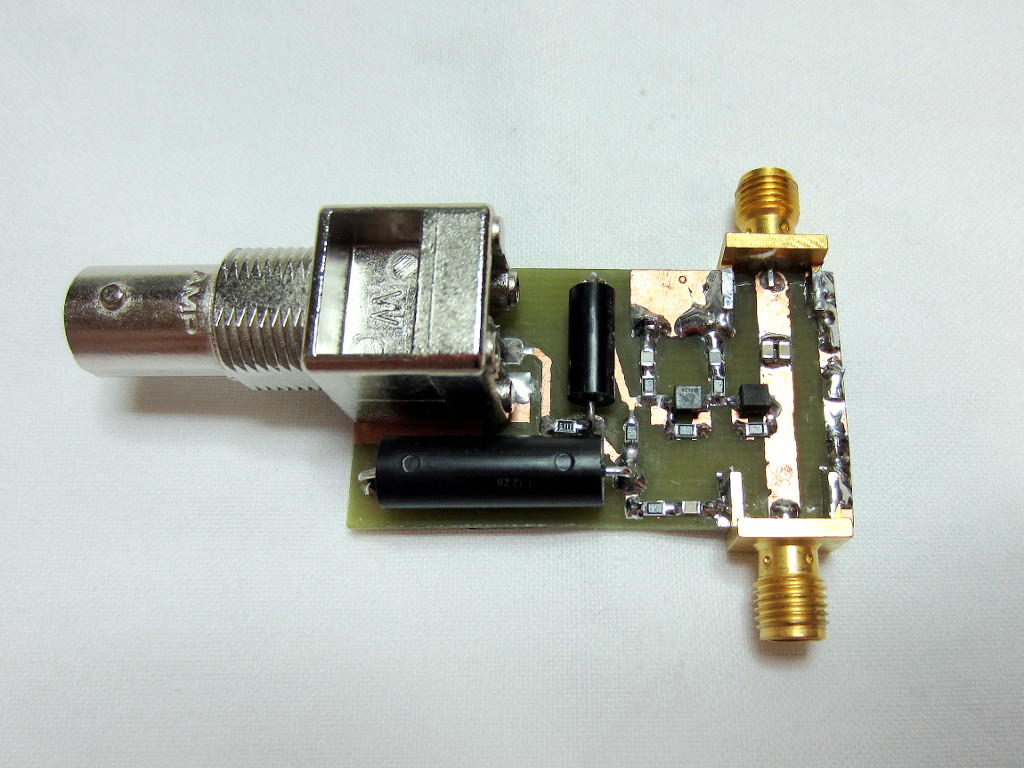
Quite some time after performing the above simulations, I found the time to finally etch a PCB (using the template provided by Gary) and assembly a bias-tee. The PCB was made using the Toner Transfer method - the first I did this way - and the results were not too bad:
Some parts were retouched with a permanent marker, since as often happens the toner transfer was not perfect everywhere. Etching was done using ammonium persulphate, also a first here, after 30 year of ferric chloride. Worked well but much slower than I was used to, but I digress.
The components values used for this bias-tee were the ones corresponding to the "v2" design from Gary. A comparison of the simulated performances vs. the measured one can be seen in the following graphs:
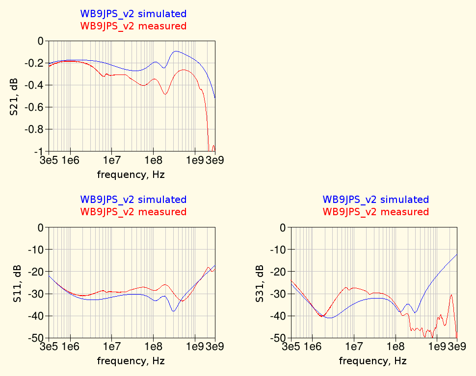
The agreement between simulations and measurements is fair, there are some more losses in the S21 at high frequency but something is not right at the lower frequencies: the shape of S21 until about 30 MHz is not right and also the isolation (S31) is much poorer than expected in that range.
The low-frequency response depends of course mainly on the higher-value inductor, L4 (470 μH) in the schematic above. A measurements of this inductor impedance vs. frequency quickly showed that the inductor self-resonance frequency was much lower than assumed, i.e. the equivalent parasitic parallel capacitance was much higher than 9 pF.
Similar measurements on the other inductors used fortunately led to measured characteristics not to different from the assumed models, at least at low frequencies.
Having separately characterized the inductors used in the bias-tee, I had then available their two-port S-parameters, which I used to to a more accurate simulation of the bias-tee performances:

In the schematic above, instead of the basic inductor models made with lumped components previously used the measured S-parameters model were substituted (SUBn components).
The simulation results of the schematic using the measured inductor characteristics are shown below, compared with the measured performances of the fabricated bias-tee:
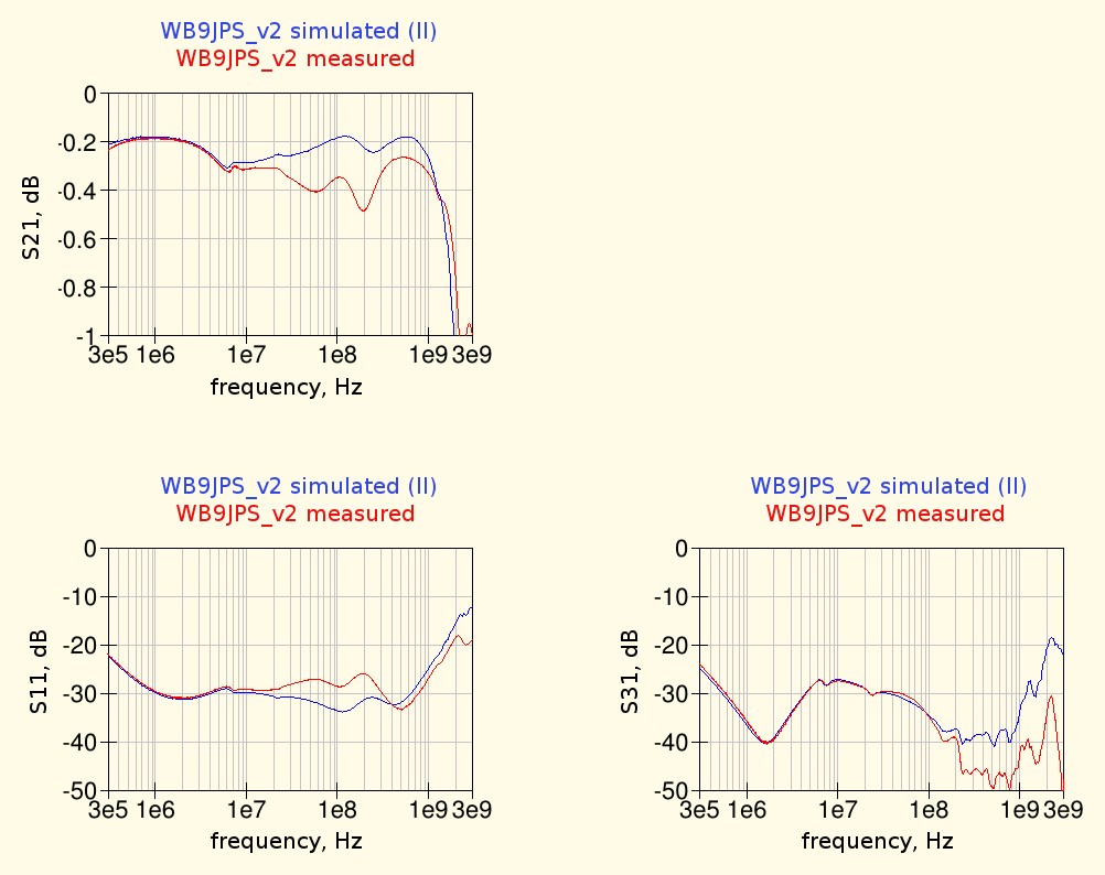
using the measured inductor data the simulations results are matching the bias-tee measurements almost perfectly at low frequency and also the high frequency response is now closer to the measured one.
Still some difference at mid and high frequencies remains; a detail that has not been taken into account in the simulations up to now is the parasitic capacitance of the components pads and traces on the PCB. Since the bottom layer is a continuous ground plane, every copper trace on the top has some capacitance to ground. While this is a desired feature for the main 50 Ω line (together with its inductance it defines its characteristic impedance), the other traces were considered as ideal, with no capacitance to ground.
With the help of an old but still perfectly working Bontoon 71 A Capacitance/Inductance Meter, I measured the PCB pads capacitance to ground; the resulting schematic with the parasitic capacitances (Cparn) is shown below:

and comparing the simulation results from this schematic with the previously measured data we obtain the following graphs:
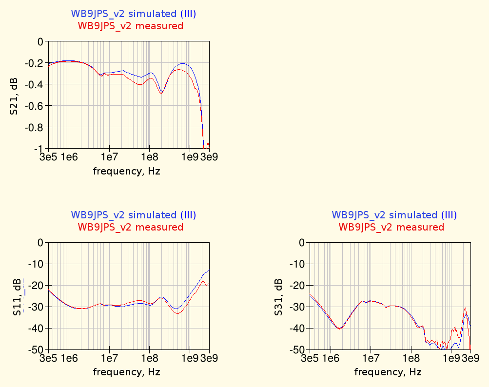
where we can see that the agreement between measurements and simulations is much improved, only some small differences remain.
Since it was now clear that even the small components pads capacitance have a detrimental effect on the bias-tee performances, I wanted to check how much improvement a reduction of these parasitic capacitances could bring.
Not wanting to do a new PCB with a different layout, the only way to reduce these capacitances was to remove the ground plane underneath the pads, still leaving the ground connected where it was needed. A simple solution was to remove a small copper rectangle on the PCB back side, as shown in the following drawing (taken from Gary's document, with some modifications) :
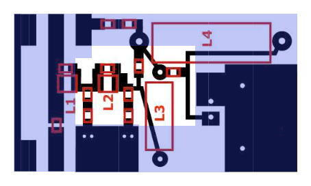
here the light blue color identifies the ground "plane" on the bottom of the PCB and the white area in the middle is where the copper need to be removed to reduce the parasitic capacitances to ground.
The problem now was removing a copper area from an already assembled PCB; this would normally rule out the usual chemical etching, but with some ingenuity this can still be used
After delimiting the (almost) rectangular area to be removed with a permanent marker (which is also resistant to the etchant), I built small "walls" around it with some adhesive putty and filled it with the usual ammonium persulphate etchant:
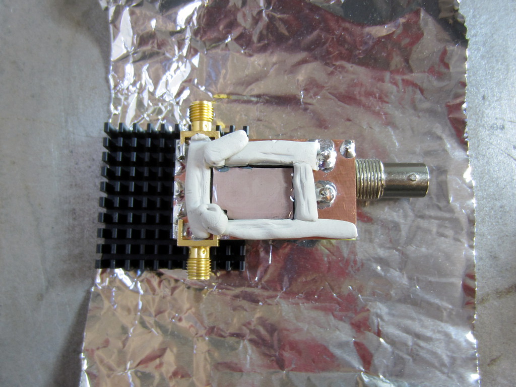
since this etchant work well only at elevated temperatures, I place the assembled PCB over an hot plate at around 50°C (the heatsink in the picture was used only as support). The etching process took some time, also because I had to change the etching solution several times, as it became quickly saturated and so unable to remove the copper anymore. In fact, googling around I learned that about 1 cubic centimetre of etchant is required to remove 1 square centimeter of 35 μm copper, so the wall should have been at least 1 cm high.
In the end the results was not too bad:
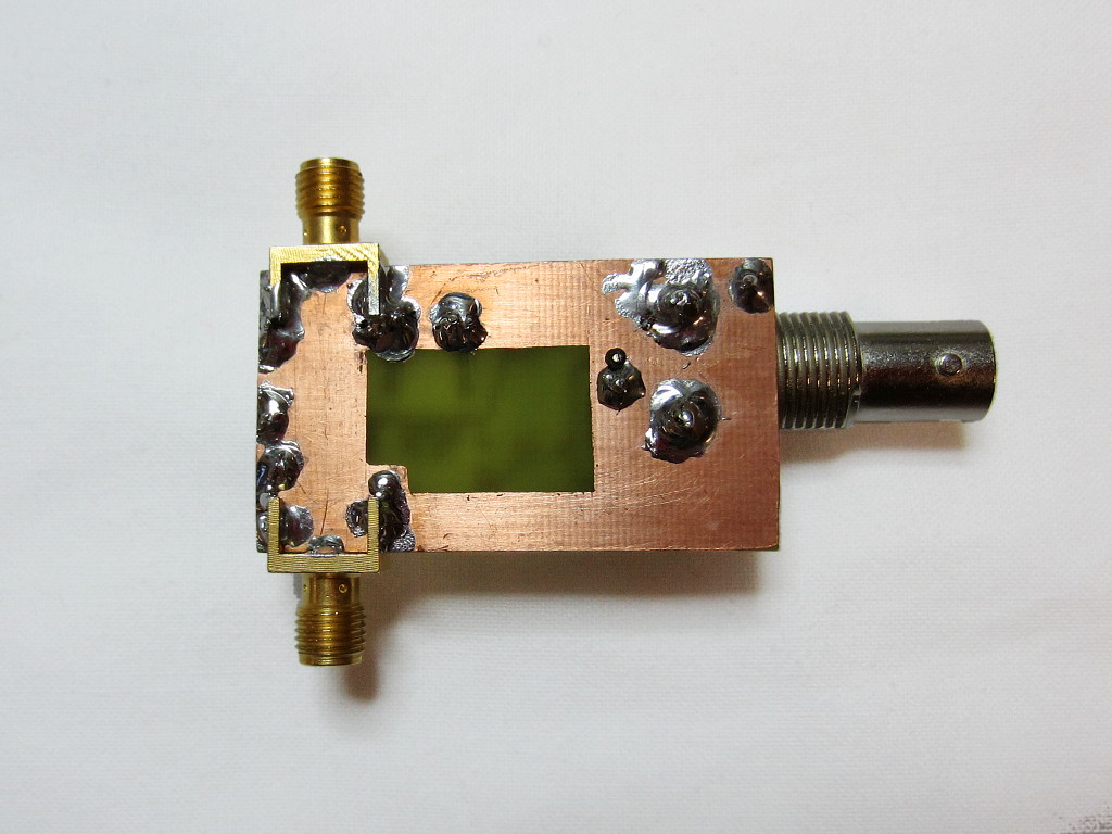
the rectangular ground area was removed and the borders delimited by the marker resisted quite well to the action of the etchant.
Here are the measured curves of the bias-tee after removing the ground plane are below the traces, compared with the original simulation results (using the measured inductors data and assuming no parasitic capacitances to ground) :
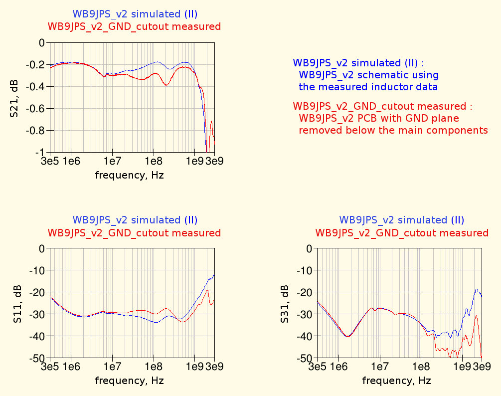
the differences between simulations and measurements at mid and high frequencies have been reduced; some difference still remains, very likely due to the fact that the measured inductors data were not taken under the same conditions. In fact during the measurements of the inductors these were not placed just above a ground plane, as they are in the boas tee, so also their parasitic capacitance to ground is likely underestimated.
So this is all regarding the analysis and optimization of the nice bias tee design published by Gary; I plan to apply the experience and the optimization scripts I developed for another design, the higher current bias-tee I mentioned at the beginning...
