IN3OTD's web site
...under perpetual construction.

Hermes-Lite SDR - AFT05MS003N push-pull power amplifier measurements
Measurements on a QRP power amplifier using a push-pull of AFT05MS003N.
This PA was a prototype for the Hermes-Lite PA.
Measurements were done for the following conditions:
- 7.5 V drain supply with frontend v1.42 as driver
- without negative feedback between drain and gate
- without compensation capacitor on the output transformer
- 9.0 V drain supply with frontend v1.42 as driver
The PA was also characterized stand-alone; for details see this page.
The schematic is a classic push-pull amplifier with resistive feedback, driven differentially by the driver board:
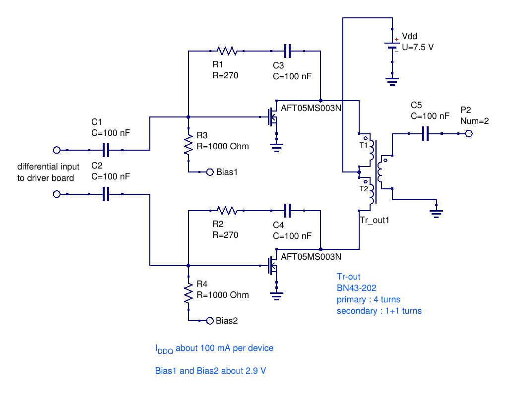
The PA output transformer was a BN43-202 binocular core with 4 turns on the 50 Ω side and 1 turn + 1 turn on the low-impedance side to the LDMOSs.
Later versions used a Epcos/TDK B62152A4X30 core with the same windings. This transformer is smaller and gives slightly better performance.
PA output at 7.5 V, frontend v1.42 driver
The following graphs show the PA performances for a power supply voltage of 7.5 V.
The PA was driven by the Hermes-Lite v1.42 driver board.
The firmware FPGA FW version used was the 20160220_txdac/CVA9/, half-duplex.
The system clock frequency fs was 73.728 MHz
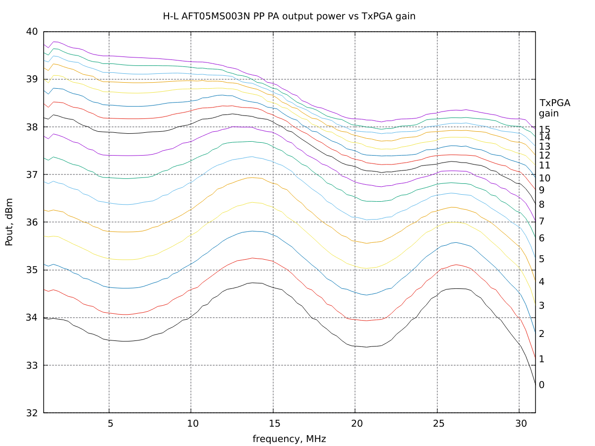
Output vs. TX frequency and TxPGA gain
PA output power vs. frequency for several TxPGA gain values (TxDAC gain, see the AD9866 datasheet for details).
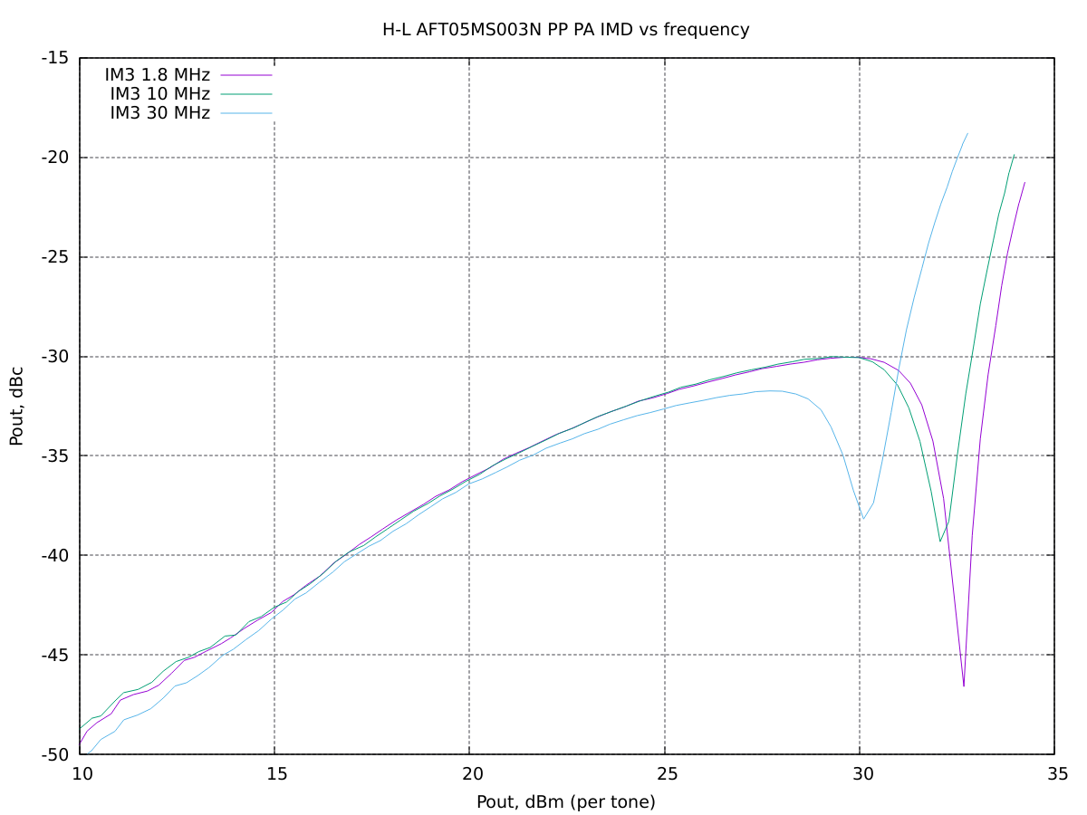
IMD vs. output power
Two-tone intermodulation distortion measured for three different center frequencies.
Output harmonics and spurs vs. frequency
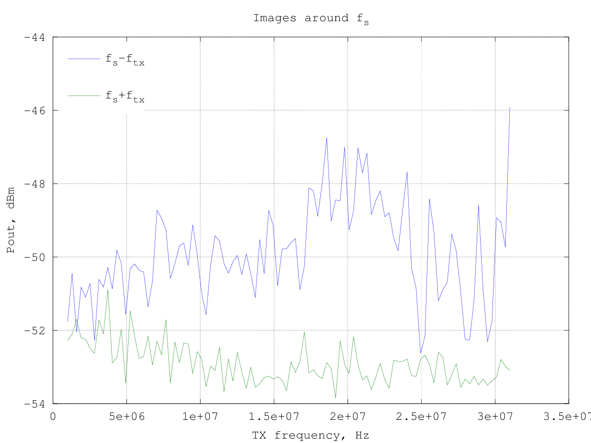
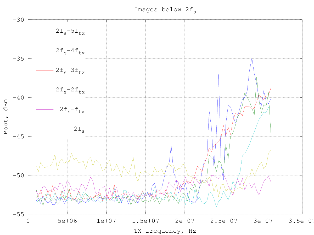
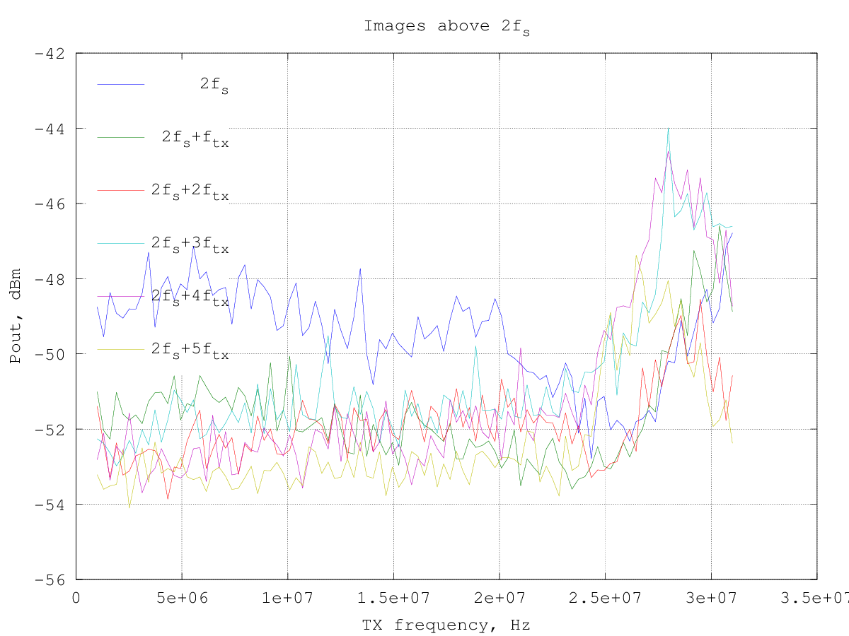
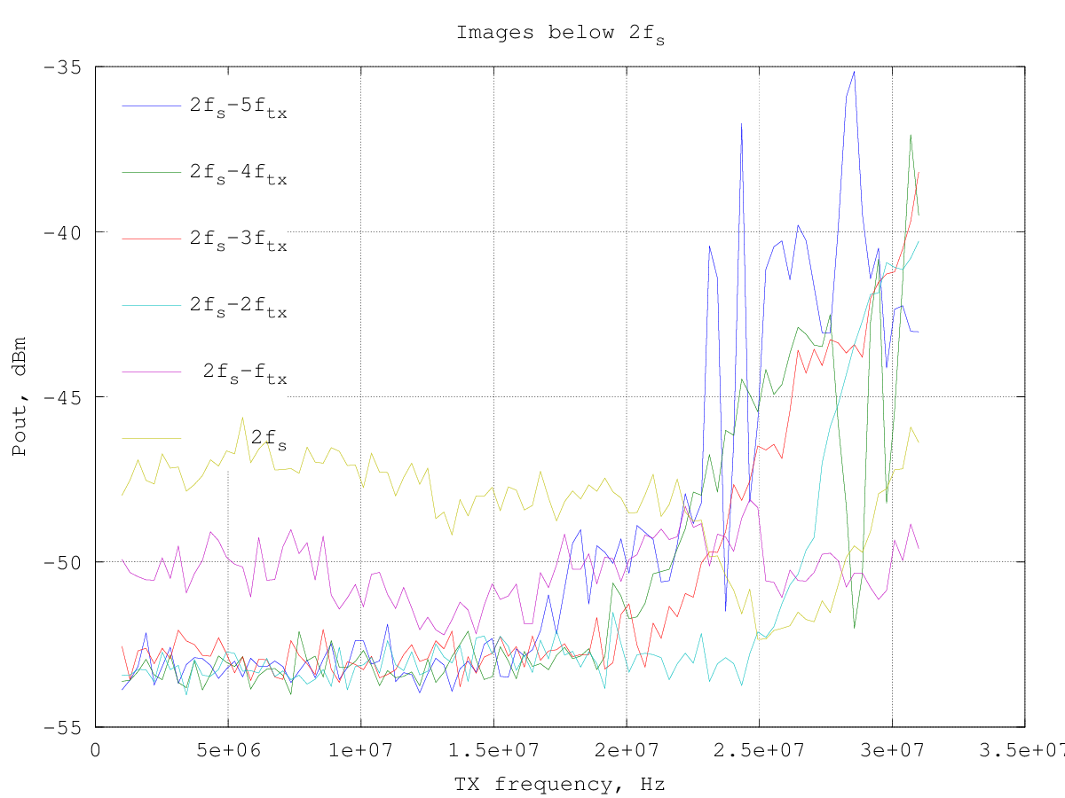
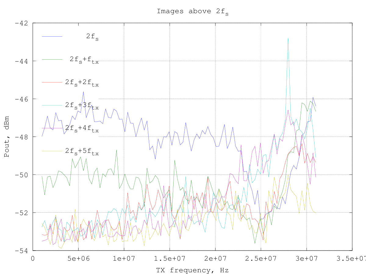
TX output harmonics, DAC spurs and images vs. frequency for a TxPGA gain setting of 6, which gives an output power around 37 dBm (5 W), see graph above.
The harmonics are mainly generated by the PA, as the AD9866 TxDAC harmonics are filtered out by the frontend filter (above 30 MHz) and the harmonics level generated by the driver is low.
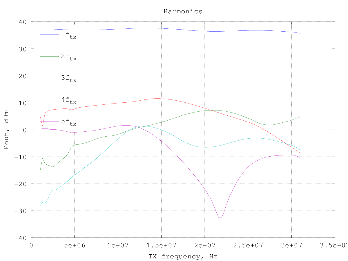
The sampling images and spurs are also mostly filtered out by the on-board filter, except of course when they fall in the filter passband. There is also some feedthrough in the filter stopband, probably due to a limited ultimate rejection.
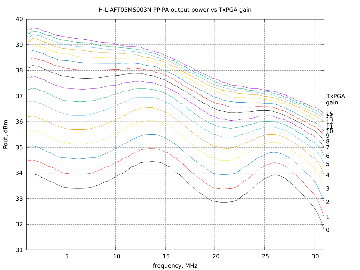
Output vs. TX frequency and TxPGA gain without compensation capacitor
PA output power vs. frequency for several TxPGA gain values without compensation capacitor on the output transformer.
Note the big power drop at the higher end of the HF versus using the optimal compensation capacitor (see graph above).
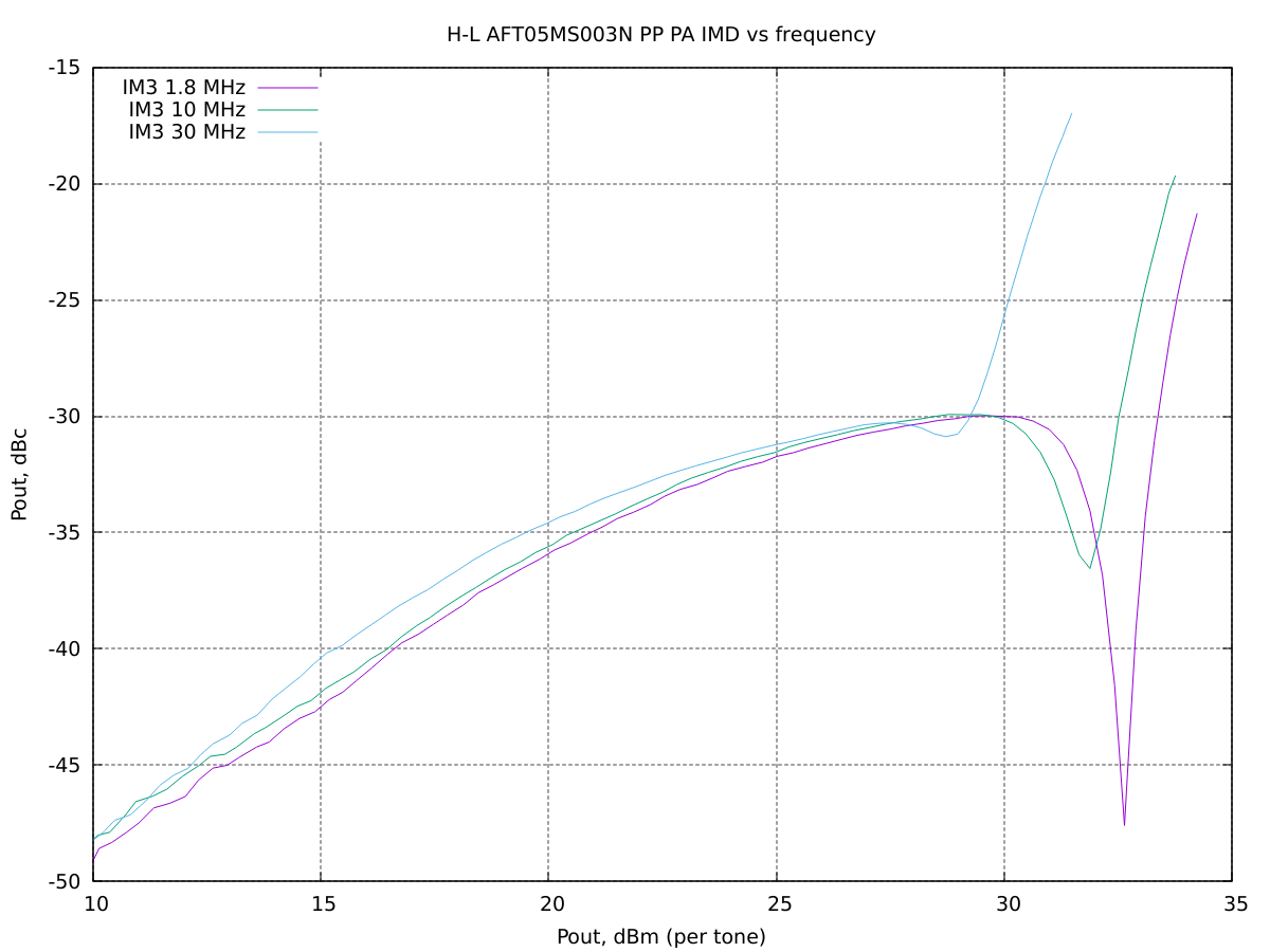
IMD vs. output power without compensation capacitor
Two-tone intermodulation distortion measured for three different center frequencies without compensation capacitor.
Except at the higher frequency end, the IMD is about the same as with the compensation capacitor.
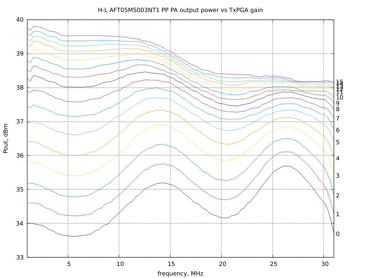
Output vs. TX frequency and TxPGA gain without negative feedback
PA output power vs. frequency for several TxPGA gain values without negative feedback via the drain-gate resistor. The input impedance was brought to about 50 Ω by lowering the gate bias resistor.
Note the apparent higher gain at the higher end of the HF versus using the negative feedback (see graph above).
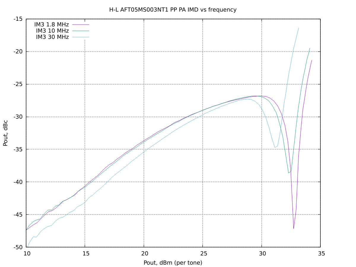
IMD vs. output power without negative feedback
Two-tone intermodulation distortion measured for three different center frequencies without negative feedback via the drain-gate resistor.
Note the much higher IMD versus the negative feedback case (see graph above).
PA output at 9 V, frontend v1.42 driver
The following graphs show the PA performances for a power supply voltage of 9.0 V.
The PA was driven by the Hermes-Lite v1.42 driver board.
The firmware FPGA FW version used was the 20160220_txdac/CVA9/, half-duplex.
The system clock frequency fs was 73.728 MHz
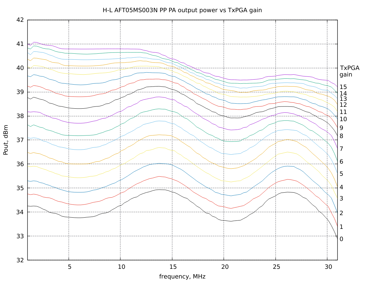
Output vs. TX frequency and TxPGA gain
PA output power vs. frequency for several TxPGA gain values (TxDAC gain, see the AD9866 datasheet for details).
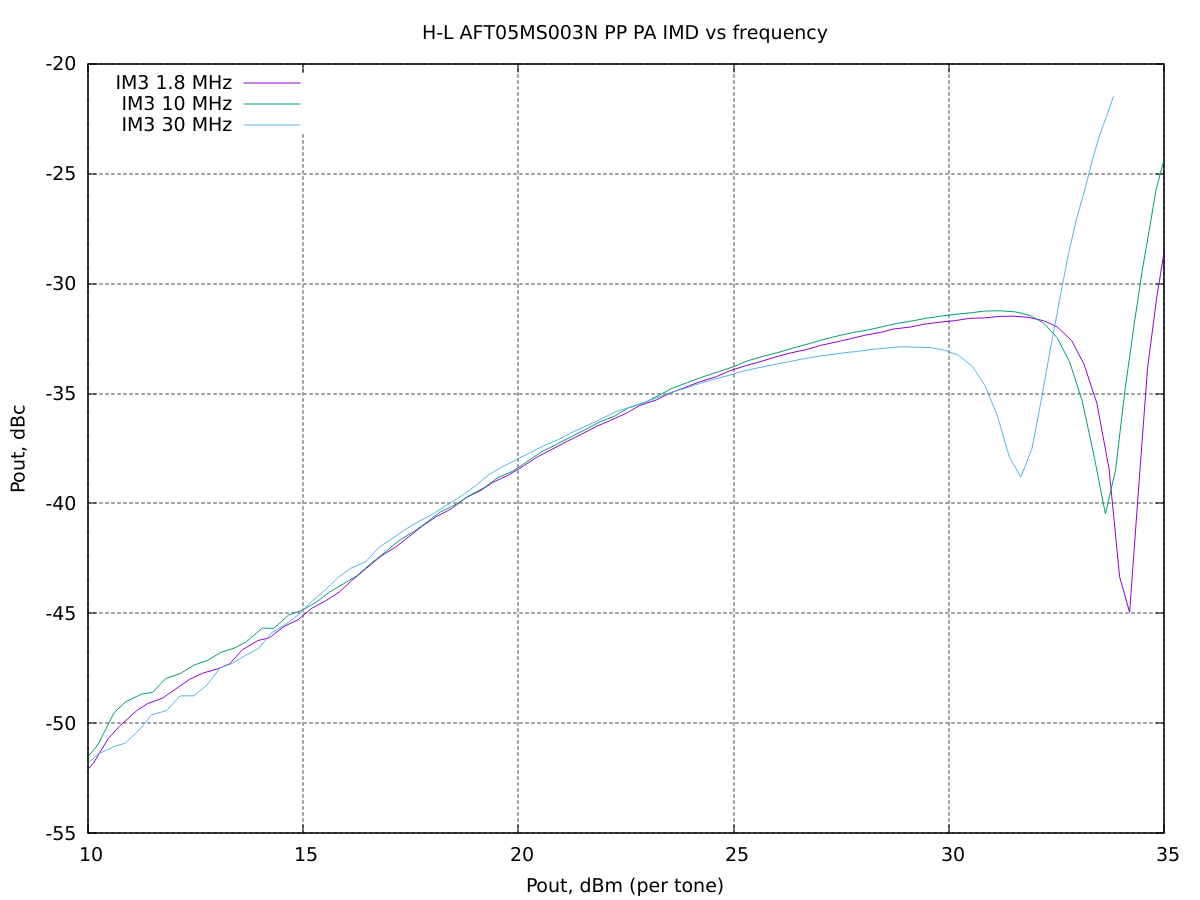
IMD vs. output power
Two-tone intermodulation distortion measured for three different center frequencies.
Output harmonics and spurs vs. frequency
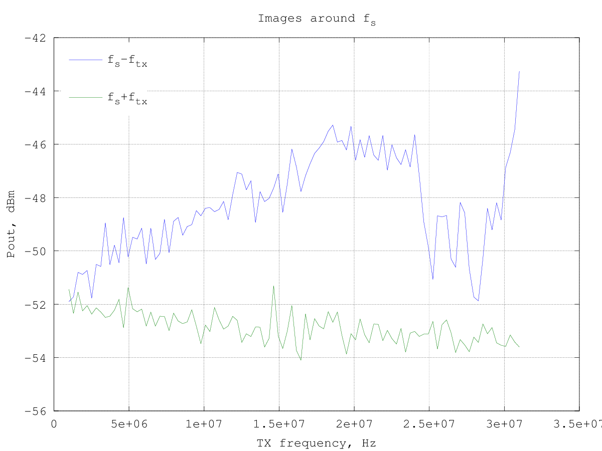
TX output harmonics, DAC spurs and images vs. frequency for a TxPGA gain setting of 6, which gives an output power around 37 dBm (5 W), see graph above.
The harmonics are mainly generated by the PA, as the AD9866 TxDAC harmonics are filtered out by the frontend filter (above 30 MHz) and the harmonics level generated by the driver is low.
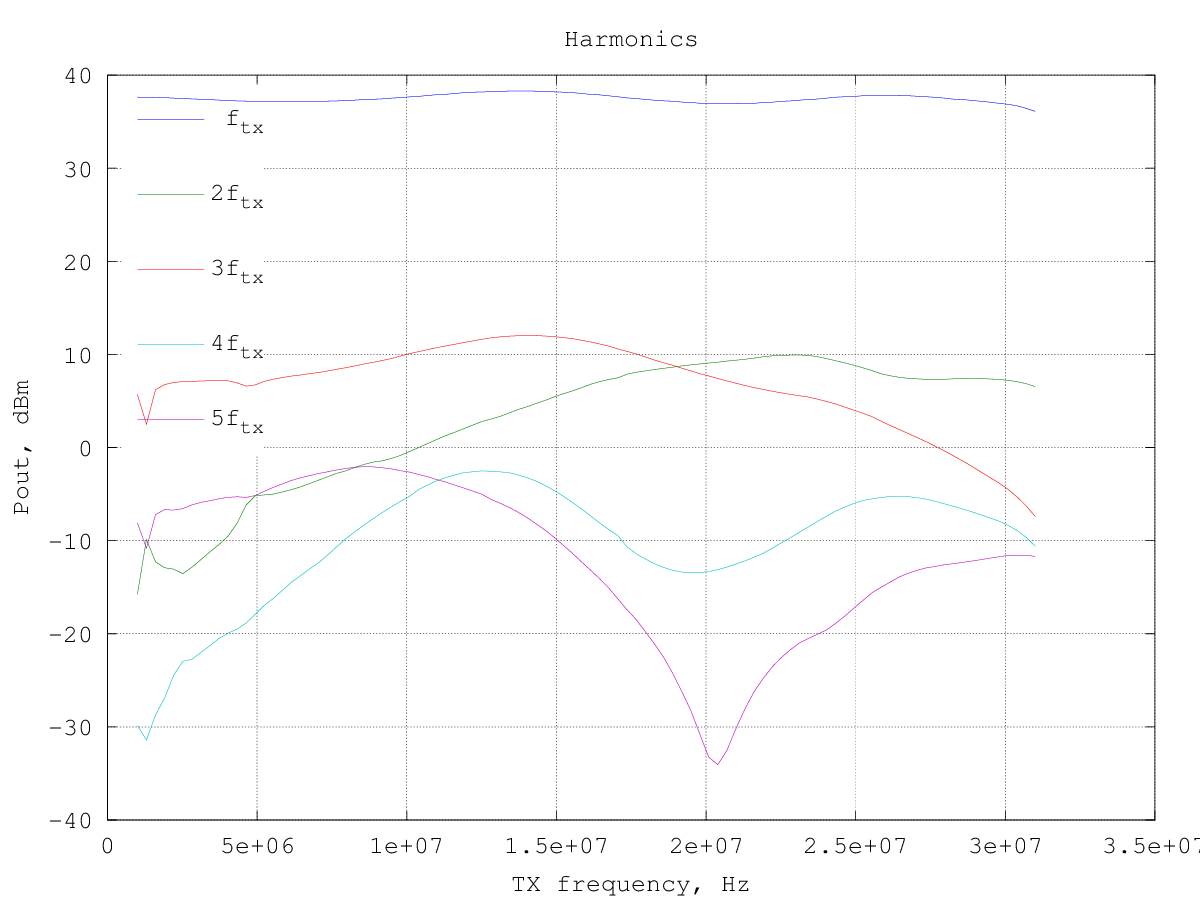
The sampling images and spurs are also mostly filtered out by the on-board filter, except of course when they fall in the filter passband. There is also some feedthrough in the filter stopband, probably due to a limited ultimate rejection.
