SHF Systems 144/902 Transverter Part 1
Happened upon a small cardboard box in the take to next ham fest tote and discovered it contained parts for a 144 MHz to 902 MHz transverter board set. Opening the box yielded one circuit board with a built-up oscillator section on it, two blank boards and a thin set of printed documentation.
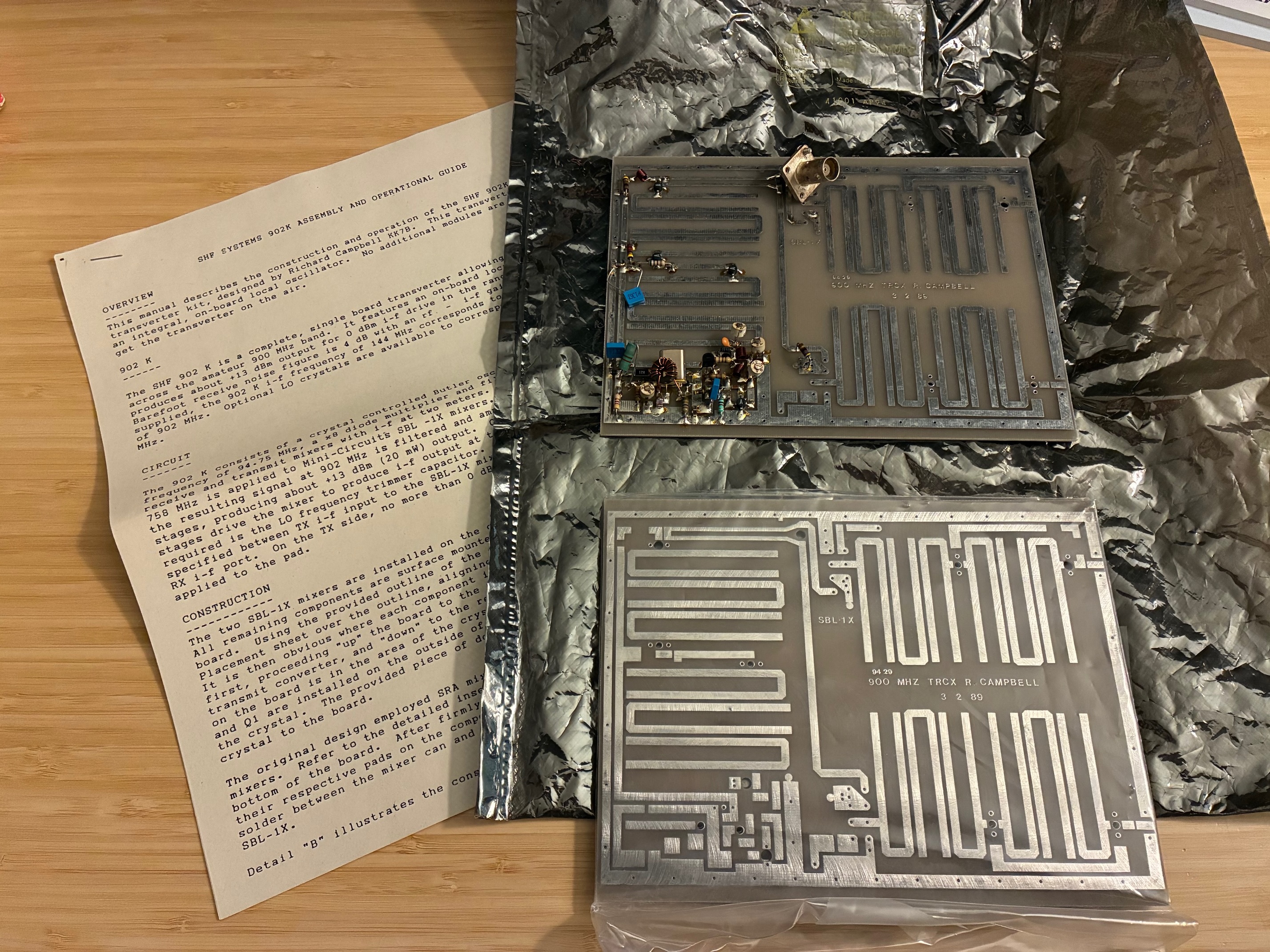
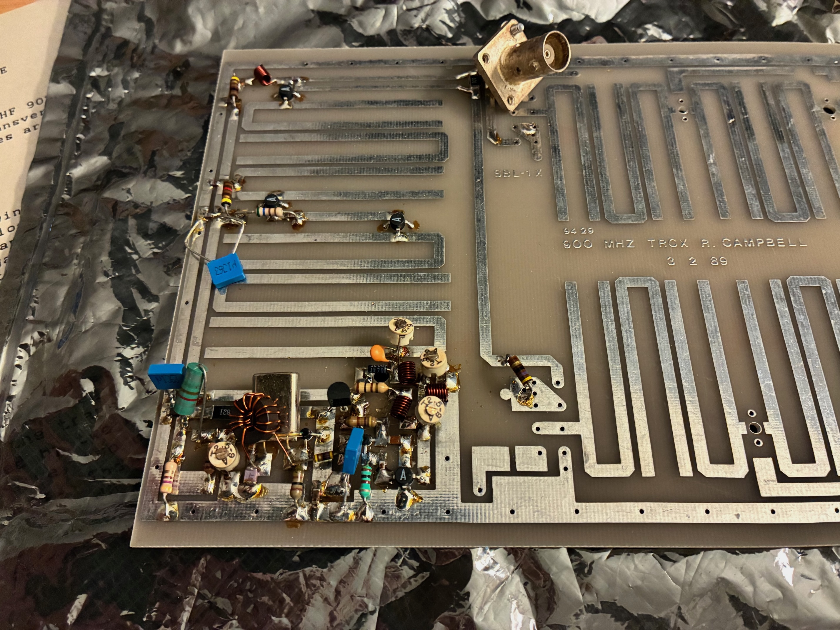
These 2 meter to 902 MHz transmit/receive converter boards came from a local Chicagoland ham who had ordered them from Down East Microwave back in the late 90's, built up the oscillator/multiplier stages on one board, (likely had trouble making it work), and then lost interest thereafter. Here are some close-ups of the parts-installed board and the blank boards.

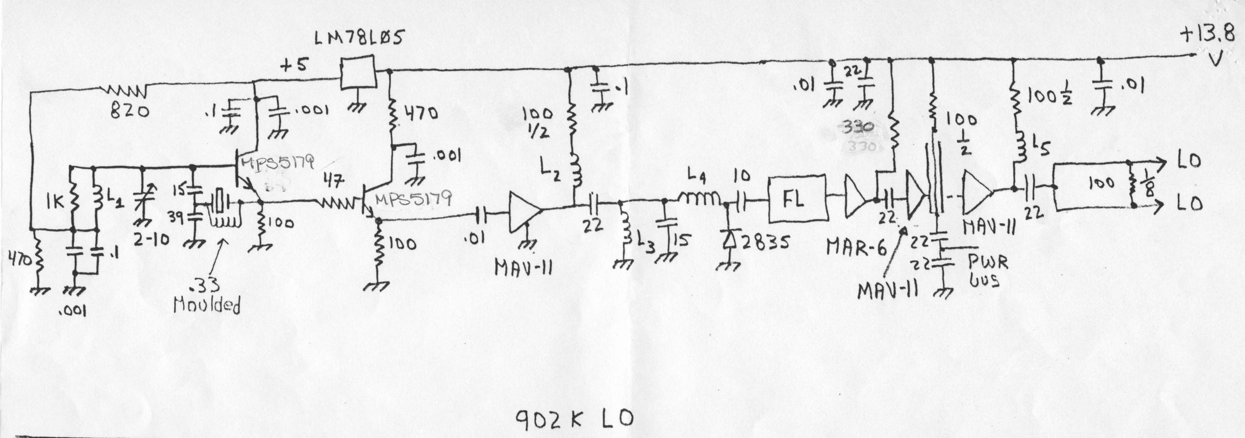
The design is by R. Campbell, KK7B and utilized on-board filter traces to provide needed filtering and isolation across the transmit and receive converter stages. Documentation is limited, with an on line manual available here. A follow-on document describing updates to the converter design was found here.
A brief search for completed examples of this specific 144/902 converter was made with little success. The manual shares that external relays, control lines, attenuators, and amplifiers are likely needed. While known top-level that these items are needed, additional time will be needed to explore these functions should a working converter be achieved.
A quick inspection of the board with the built-up oscillator section shows a few differences between the documentation and the as-built unit. For example, a moulded inductor was specified in the design documentation, while a wound toroid coil is actually present across the crystal on the partially built-up board. Several MMIC amp bias resistors are not as specified on the schematic. And, all of the MMIC amps have the same capital "A" marking on the top of them, compared to two different amp types being called out in the schematic. These difference point to proceeding cautiously and closely inspecting each stage during the checkout process.
Initial Checkout and Tests
The schematic showed +13.8 VDC as main power input with an on-board regulator down to +5 VDC for the crystal oscillator and buffer amplifier. Cautiously applying a +12 VDC supply to the board showed it was consuming ~ 208 mA at that voltage. Given the presence of six active devices (two transistors and four broad-band MMIC amplifiers), this seemed reasonable.
With power applied to the board and the TinySA-Ultra RF spectrum analyzer connected to the BNC jack at the RX SBL-1X mixer location, the following spectrum was observed. (Was looking for 758 MHz at about +7 dBm to drive the SBL-1X mixer.)
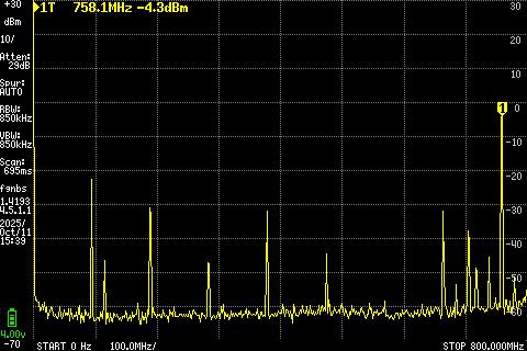
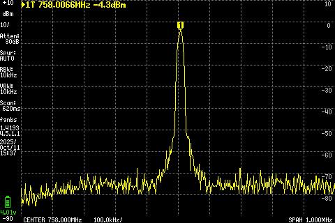
Zooming in a little showed that the oscillator is reasonably on-frequency but still low in signal level. Overall, a good start with 1) oscillator working, and 2) multipliers from crystal frequency up to 758 MHz working.
Looking over the schematic points to checking out each stage to see if one of the stages is not working as needed. The oscillator is oscillating and the follow on buffer buffering, but likely one of the following amplifiers is not giving the needed gain to provide the +7 dBm LO output power at the mixers.
Setting up to measure RF spectrum and power level at each of the stages involved use of the Agilent/HP-1121A RF probe feeding the TinySA-Ultra analyzer. Previous posts for the HP-1121A probe are here (functional test) and here (bandwidth check). Today's test setup to measure RF stage levels is below:

The +12 VDC power is applied via the red and black clip leads, and the HP-1121A probe connects in by touching points in the circuit with the probe tip (used with the short ground lead), with the probe output connected to the TinySA-Ultra via a SMA DC block and RF adapters. (Actual measurements had the 10X attenuator added on the probe tip - wanted to be extra careful with the RF probe until comfortable using it in the home lab.) Measurements were taken at the amplifier inputs and outputs to see if all stages were providing gain. DC voltages at amplifier input and output are captured just above the amplifier symbols. Measured RF levels (SA marker readings) are written in groups just below the amplifier symbol on the schematic copy.
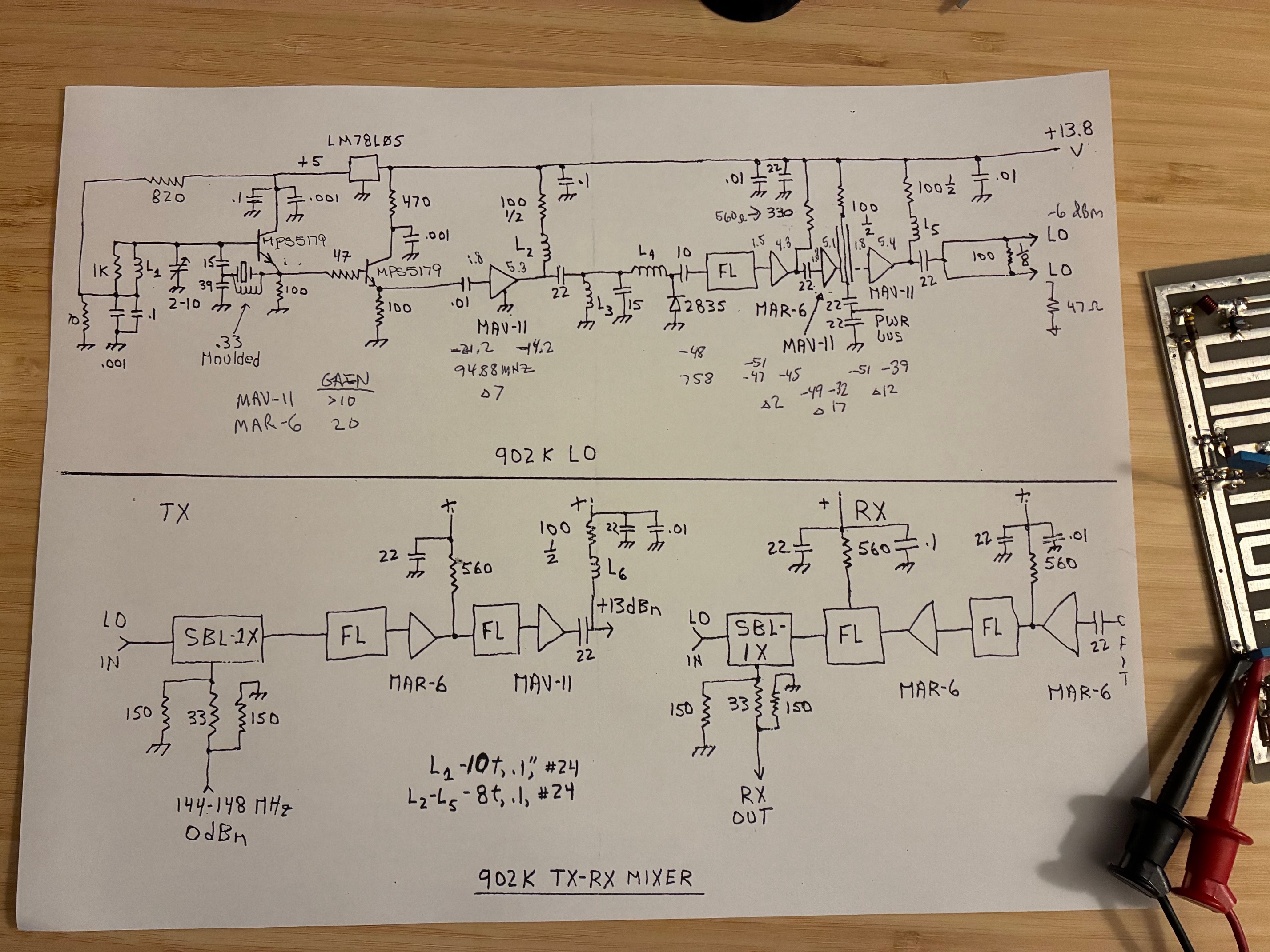
The first amp stage looked good for both DC and RF levels, providing ~7 dB gain between input and output. The second amp (MAR-6 on schematic) only provided ~2 dB gain and had low DC levels compared to other amps in the line up. The last two amplifiers looked OK for DC and RF levels. The second RF amp seemed to be having trouble amplifying the LO signal.
Closer visual inspection of the amplifiers, and in particular the second amplifier showed a 560 Ohm bias resistor instead of the 330 Ohm value indicated on the schematic. Given all the MMIC amps are the same top-marking (capital A), one might expect they would all use the same value bias resistor (100 Ohm installed/used for the other three MMIC amps).
With all of the installed MMIC amps having the same "A" marking, a search for parts with that marking was conducted. After around 20 minutes (and ~100 pages viewed), an early version of the Mini-Circuits MAV-11 data sheet was located indicating "A" marking for that component. For reference, later MAV-11 data sheets indicate a "-11" marking for the component. Knowing the specific part used will help in straightening out the bias resistor value jumble (multiple installed values not matching each other, or the schematic values).
Next Steps
Will find a 100 Ohm 1/4 watt resistor and replace the 560 Ohm bias feed resistor at the second MMIC in the line up. Hoping further tests will show closer to +7 dBm at the soldered-on BNC jack at the output of the two-way power divider circuit.
Achievement unlocked: 144/902 Converter board powers up, draws reasonable current, MMIC component identified as MAV-11, and the board produces 758 MHz LO signal (not smoke) at the BNC test jack!
Will update this post in the future...
All author photos captured with an iPhone 16e.