TinyGTC Input Protection
The TinyGTC is a low cost USB GPSDO (GPS Disciplined Oscillator), Timer, Counter that provides MANY functions and capabilities. The price point and small size forced a limitation on the input range and protection levels for the unit's three signal input circuits. Accordingly, the developer's website for the instrument includes multiple cautions against overloading the inputs and states that they have a low damage threshold compared to commercially available counter/timers by the big test equipment suppliers (HP, Tektronix, Fluke, Rohde & Schwarz, etc.).
My previous posts on the TinyGTC instrument cover Unboxing and First-Use.
The developer's recommendations for protecting the inputs includes this guidance:
- Always keep a DC block followed by a 3 dB attenuator on the A and B inputs when trying to measure an unknown 10 MHz source
- Always keep at least a 6 dB attenuator on the input when trying to measure a unknown 1 PPS
- Use a X10 scope probe followed by a DC block and a 3 dB attenuator for initial probing in a high voltage environment
- Consider using a H field sensor ( inductive pickup) or E field sensor ( capacitive pickup) to probe the output of high power sources
I am fortunate to have a selection of DC blocks, SMA coaxial attenuators, and probes and have been following this guidance, including adding some SMA RF limiters used for a few higher power RF measurements. Unfortunately, while the size of the TinyGTC itself is small, the addition of 5-6 extras takes away from the just-setup-and-use utility I was looking for. The challenge is that there appears to be no one-size-fits-all uses add-on for input protection. I found that the RF limiters worked well for protection against high RF levels, but that they distorted logic level signals such as the 0 to 3.3V 1 PPS output available on the TinyGTC OUT port. Similarly, the "choose the correct attenuator" and "do I need a DC block for this input" tasks just made the whole thing a little more complicated than I wanted to deal with. Simple is good (if it works!).
The question is if there is a simple add-on that could just be left on the two input ports A & B, and not have to worry about what type of signal is being applied? This post explores that opportunity.
Off the Shelf Solutions
TAPR sells a RF limiter in their on-line store. This is a nice option at $20 USD each and provides a fusable limiting resistor and back-to-back diodes limiting the output to less than 1 V P-P at the output. For me, the only limiting factor is that I might need three of them, and there is always a DC block in the RF path (not needed or wanted for some applications).

For just adding input RF signal limiting such as on the front end of an SDR, this is a great solution. It even has spare resistors on board that can be selected if you happen to zap it with a transmitter keyed up into it.
KiwiSDR.nz offers a receiver protector for their KiwiSDR receivers. This also has a fuse and includes a 3D printed case. These are offered at $28 USD with free shipping.


Having found these two options and being not excited about spending $60-90 for a trio of them, I figured it might be worth it to just put together a simple design and see how it worked with both RF and DC pulses/clocks on the TinyGTC.
Start with Simulation
Let's explore a few circuit topologies to see if any obvious solutions appear. Reading through some old HP application notes on their counter timer products yielded a simple input protector example for a 1 Mohm input. This consisted of an input series resistor leading to a shunt capacitor in parallel to a pair of back to back signal diodes. (Fundamentals of Time Interval Measurements, Application Note 200-3)

The application note included this text on page 19: "When working with a transducer such as a tachometer generator which has an output proportional to rotational speed, the simple external limiter shown in Figure 8 is effective in preventing counter overload for a signal that varies over wide amplitude limits. When using this circuit, the source always sees a minimum load of 22K at the input to the limiter so ringing and other distortion is not a problem. When working with low frequency sources (below 50 kHz) such as tachometer and flowmeter pickups C1, in the range of 100 to 500 pF, keeps high frequency noise from causing false triggering. The input signal is symmetrically clipped as amplitude increases so the trigger point of the counter must be set between ±0.5 volts."
Firing up LTSpice showed that such a circuit would indeed protect against a wide range of over-voltage conditions with minimal distortion to the clamped signal. I decided to lower the resistor value and eliminate the parallel capacitor to see how it worked out. Simulations looked pretty good, but still didn't completely define the protector circuit. Should there be a DC block in the circuit, and where specifically should it be located? What is the best series resistor value to use for expected input voltages? Would the TinyGTC reliably count on the plus/minus 0.6 VDC clamped signal level?
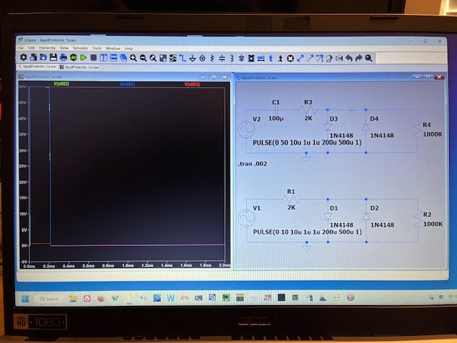
For the simulation snapshot above, the large 50V input peak signal is in blue and green (the two sides of the input capacitor in the upper circuit) and the output clamped signal is the much smaller red trace). With a 2 Kohm 1/4W series resistor, the diode current when clamping is well within the capability of a 1N914 or 1N4148 signal diode. The upper circuit adds a series DC block (AC coupling capacitor) while the lower model omits that component.
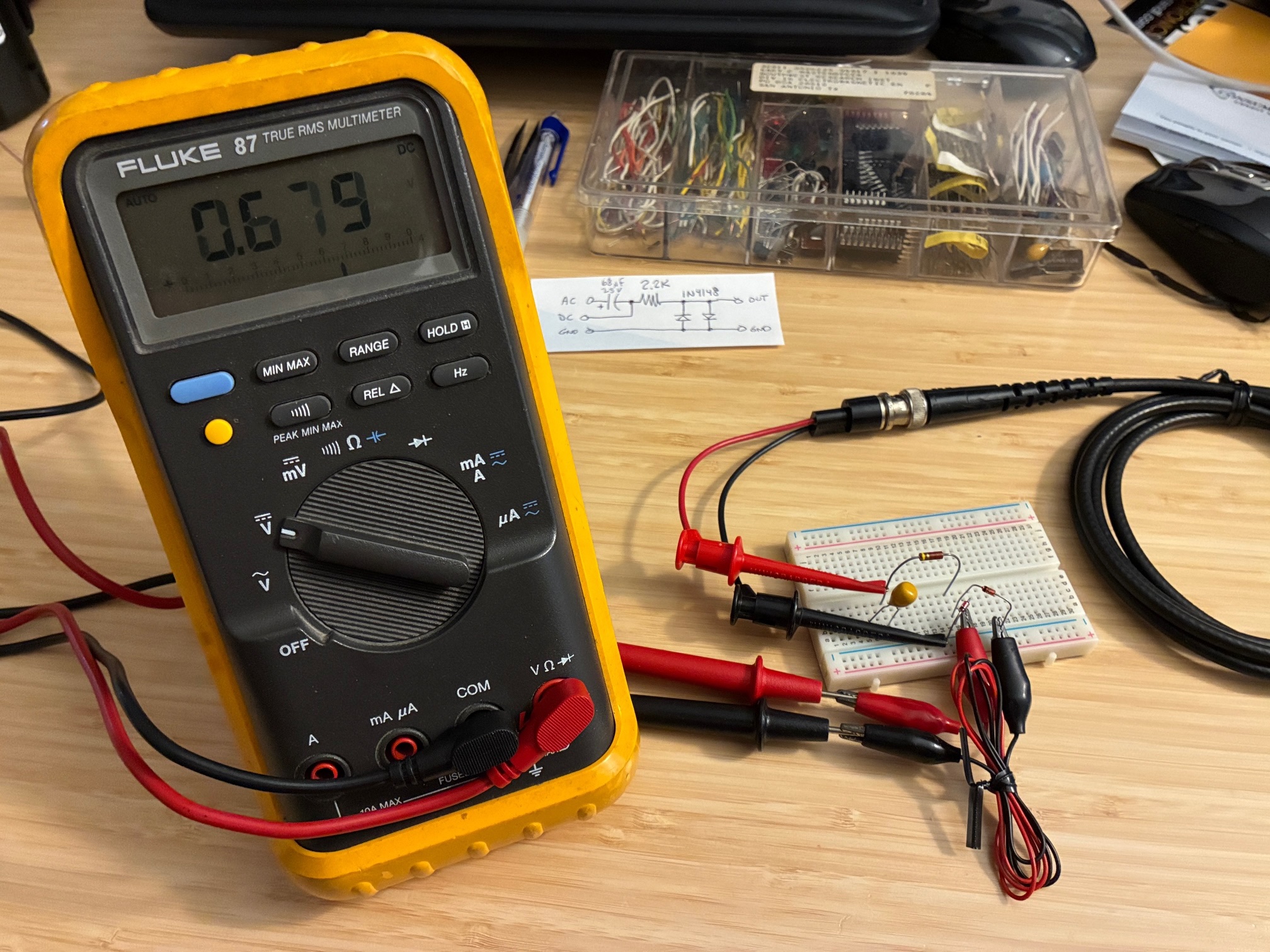
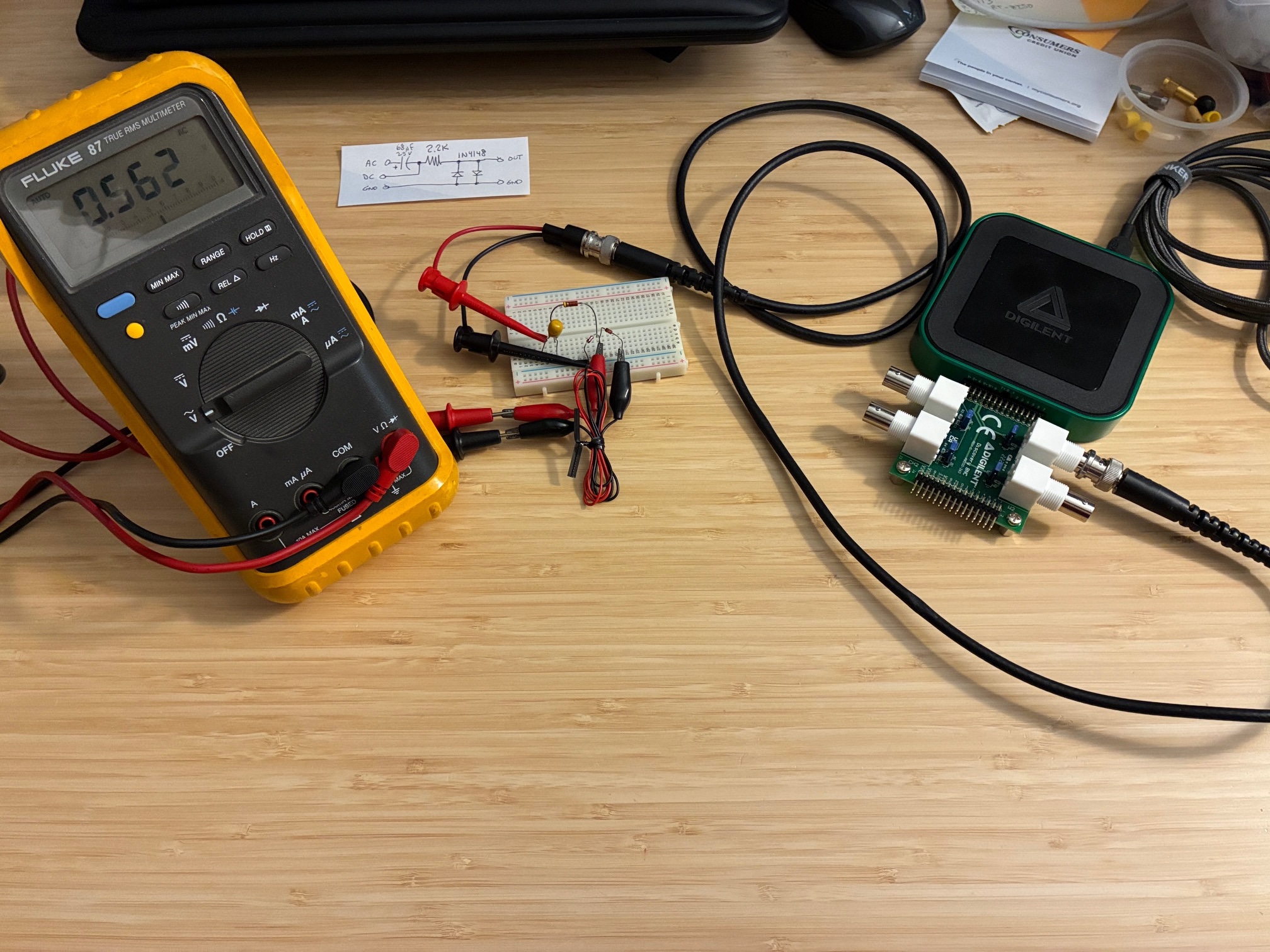
Let's build a circuit and confirm the expected operation of the clamping circuit with a few easy tests. Will use simple clip leads to hook up to the input connections and the output.
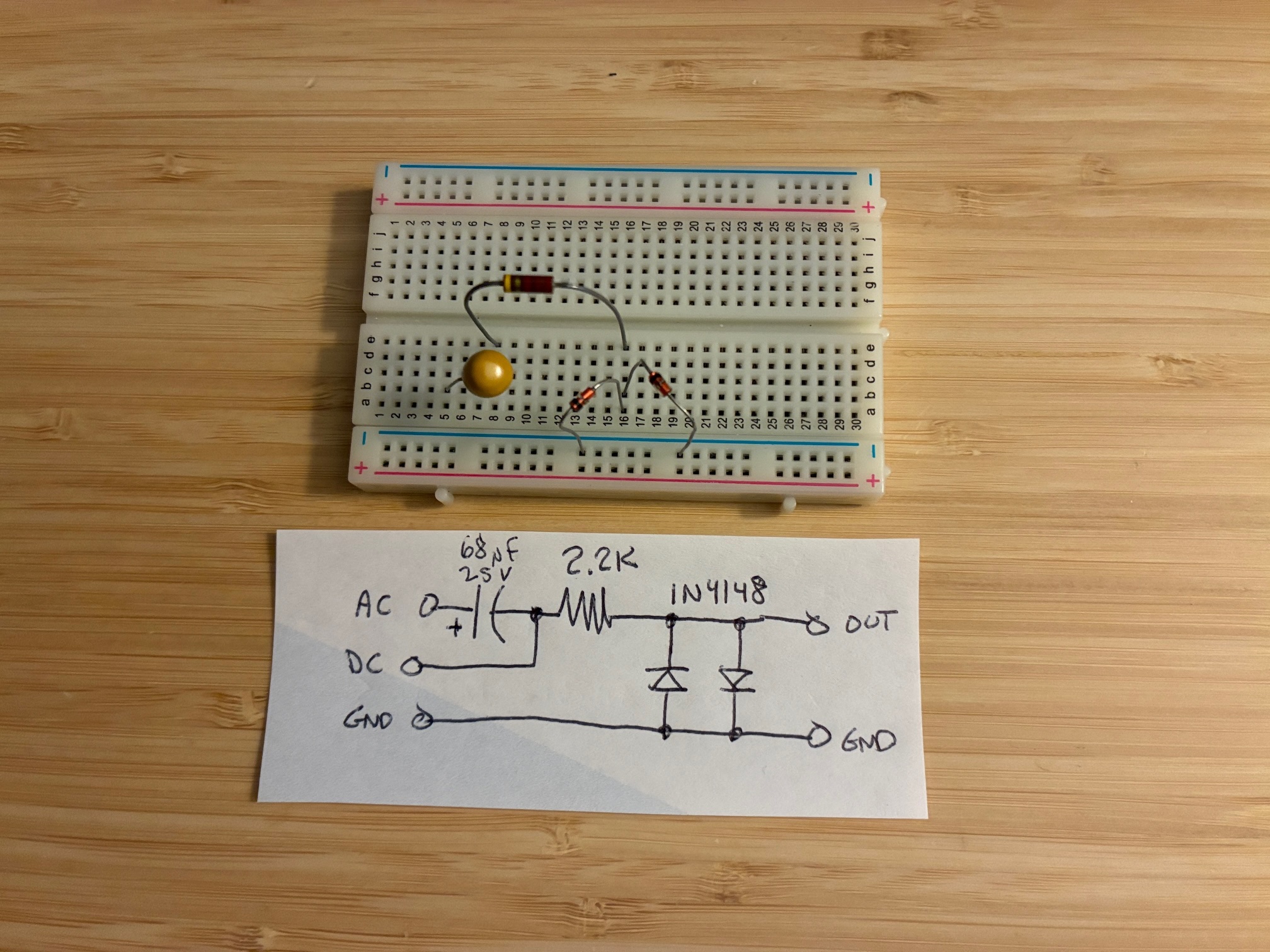
The first test just applied a +12V DC power supply to the input resistor (bypassing the capacitor) and monitored the diode clamping level. As shown below, this looked pretty reasonable at +0.679 output for +12V applied input voltage.
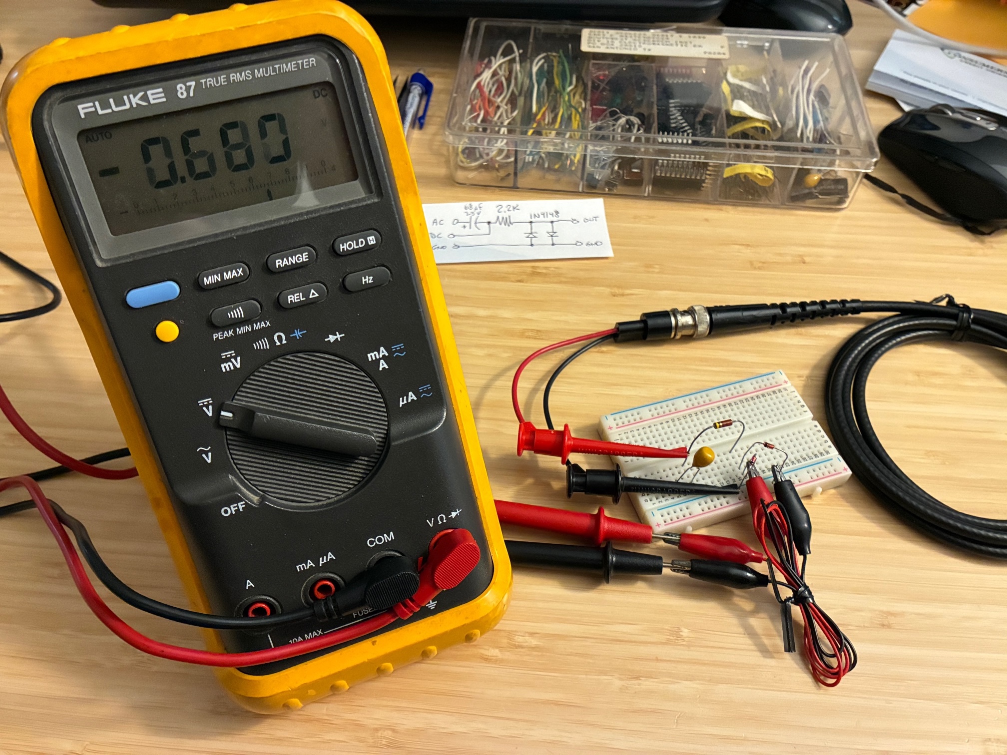
Flipping the input polarity to -12 VDC, yields -0.680 clamped output voltage. No surprises here.
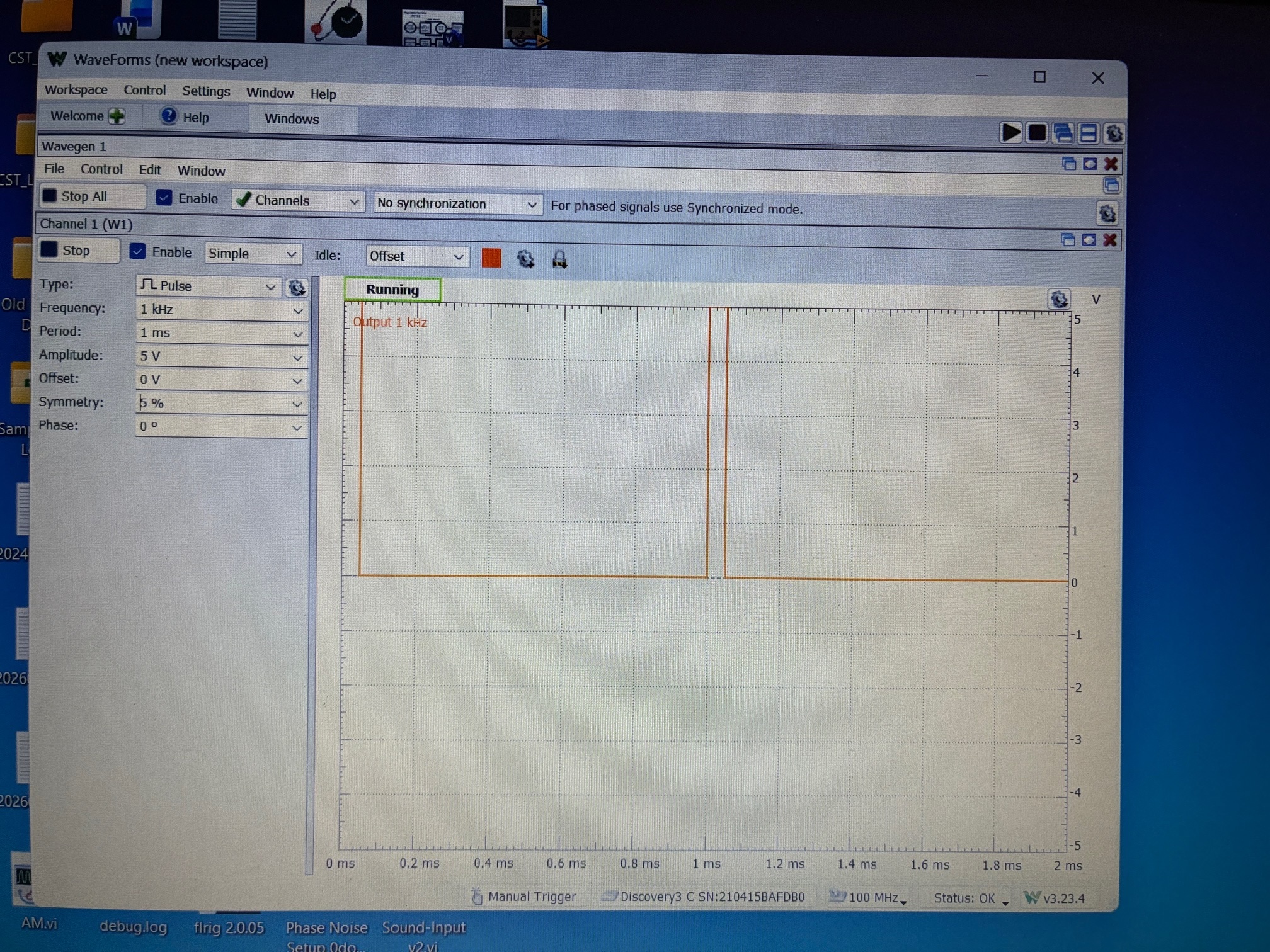
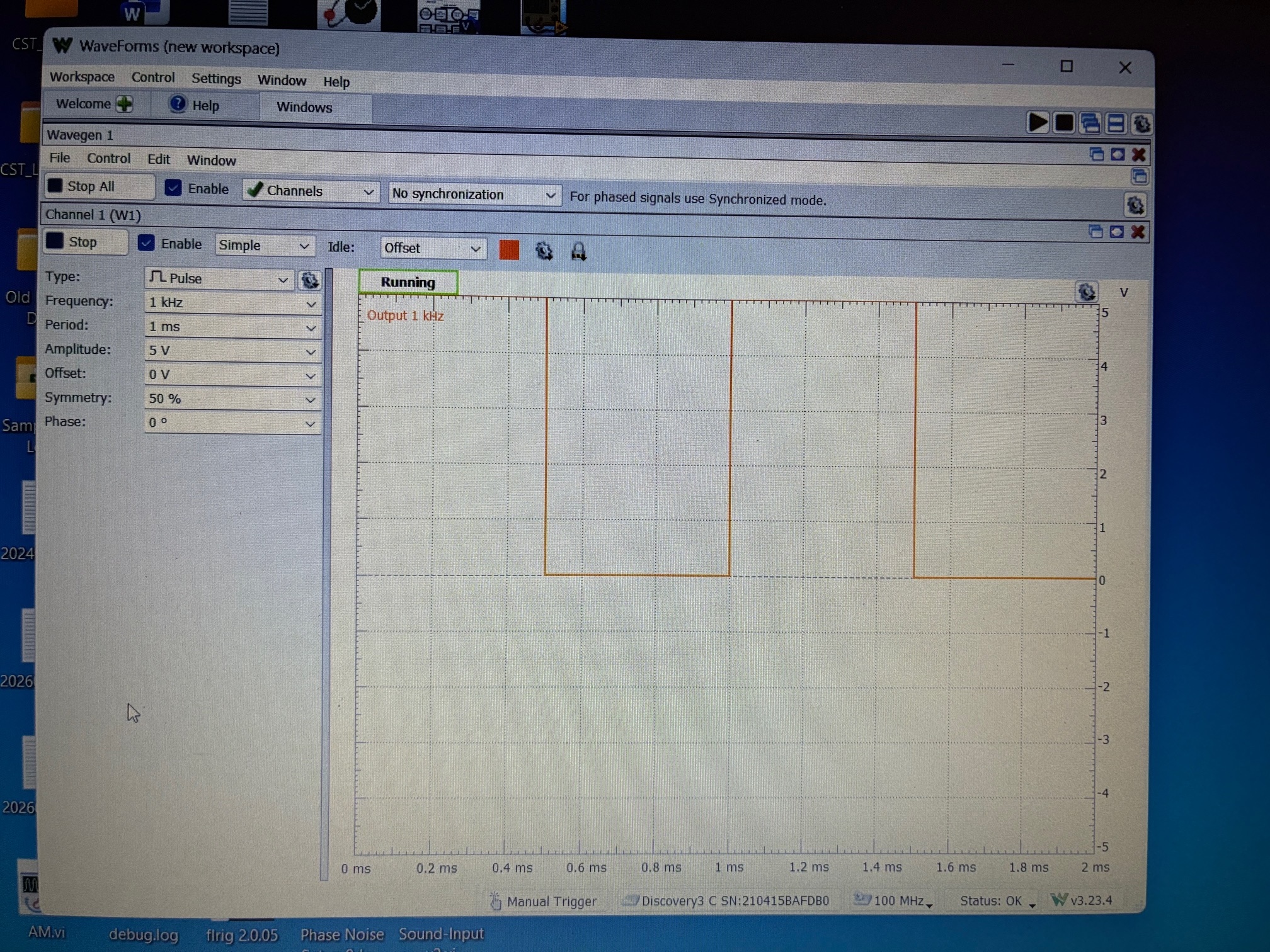
The next test applied an 1 KHz AC signal to the circuit (it worked as expected limiting 3.1 VAC RMS to 0.589 VAC RMS) and then switched to a square wave clock (0 to +5V) on an output from the Digilent AD3.
The test data for the square wave changed as the duty cycle was changed from 5% to 50% on the AD3 output. Not too much to see in the Waveforms control panel. Test data for a 1 KHz square wave is presented in a table below.
| 5% Duty Cycle | 50% Duty Cycle | |
| Input | 1.02 VAC | 2.375 VAC |
| Output | 0.226 VAC | 0.569 VAC |
The circuit works as expected, providing an amplitude limiting function to applied input signals. But will the output amplitude from the two back-to-back diodes be strong enough to be read by the TinyGTC?
The photo below shows the TinyGTC providing a 1 PPS output signal to the AC-coupled (DC blocked) input to the limiting circuit and the diode-clamped output being fed into input A. It works!
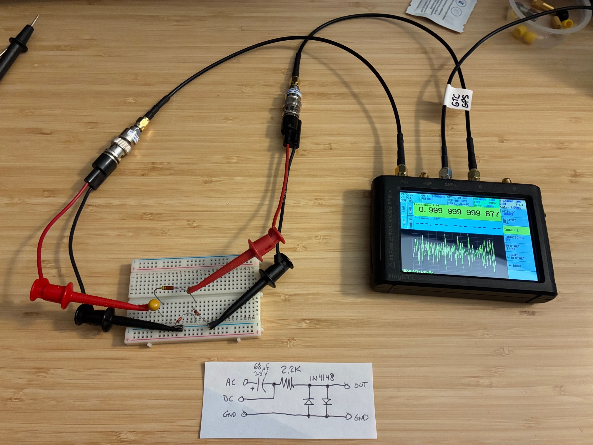
I still have a few more tests to run before calling this a success, but so far, so good. I plan to build up this circuit on a small chunk of double-sided PC board with SMA-F jacks for input output connections. While this circuit is intended primarily for lower frequency (and 1 Mohm input impedance on the TinyGTC), the performance into a 50 Ohm impedance is also of interest. After the on-board version is built, will test further - including S21 frequency response tests up to 1.4 GHz using the NanoVNA-H4 and input S11/VSWR tests up to ~ 6 GHz using the CMT R54 vector impedance probe. If that all checks out, I plan to buy some SMA-Male PC connectors to be able to just add it in-line like the two commercially available versions offer above.
Today's tests show the possibility of having just one protector type on the TinyGTC inputs. Failing that, plan to have the resistor to clamping diodes version available for the 1 Mohm impedance (1 PPS, etc.) uses and keep the RF DC blocks and SMA attenuators nearby for the higher frequency measurements. Too early to tell at this point, so will continue on the current path to a connectorized prototype clamper...
More TinyGTC RF and counter/timer fun ahead (soon with added input protection against overload/damage)!
All author photos taken with an iPhone 16e.